开漏Open Drain 和 推挽Push Pull 输出 (RT)
开漏Open Drain(开集Open Collector)
开漏输出:输出端相当于三极管的集电极,要得到高电平状态需要上拉电阻才行,适合于做电流型的驱动,其吸收电流的能力相对强(一般20mA以内)。
栅极输入 0 时,NMOS 的漏极和源极导通,输出0。
栅极输入 1 时,NMOS 不导通,漏极高阻,输出1(需要外部上拉电路,上升沿比较缓慢)。
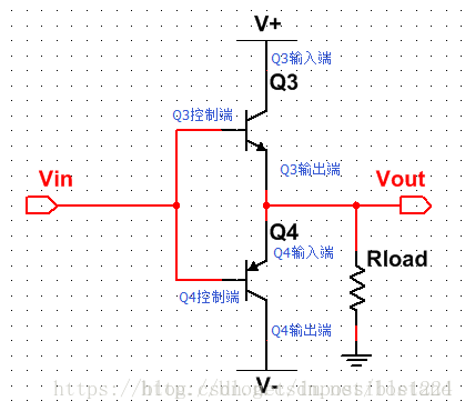
推挽Push Pull
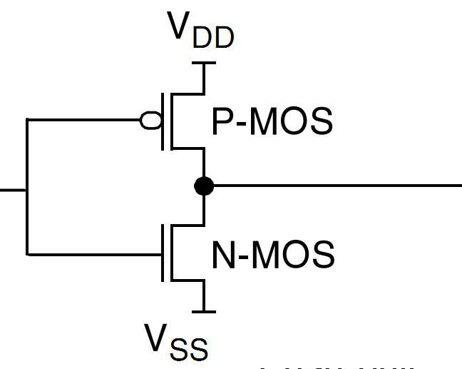
推挽输出:可以输出高,低电平,连接数字器件。
栅极输入 0 时,高侧PMOS 高阻,低侧NMOS导通,输出0。
栅极输入 1 时,高侧PMOS 导通,低侧NMOS高阻,输出1(不需要外部上拉电路,上升沿比较陡峭)。
another one:
Open Drain Output vs. Push-Pull Output
https://open4tech.com/open-drain-output-vs-push-pull-output/
Microcontrollers use pins for interfacing with the outside world. In general, the pins are the physical points on the package of an integrated circuit (IC)where a connection can be made to the printed circuit board. Behind each pin (inside the IC) there is a special circuitry used for driving it. This circuitry (usually called a pad) can be configured to allow the pin to interface with different types of digital and analog circuits. Choosing the proper pin configuration is an important part of designing an embedded system. In this article, we will cover the most common types of output configurations and their applications.
In order to explain the specifics of each output configuration, we must first introduce the following terms:
High impedance (High-Z, Hi-Z) pin -A pin that is characterized by having a high impedance which effectively removes its influence on the electrical circuit it is connected to. It is not actively driven and is “floating” unless another external device or circuitry (pull-up/pull-down) is driving it.
Floating pin – A pin is “floating” if it is left unconnected and is also not driven by a circuit inside the integrated circuit. Its voltage level is undefined and unpredictable. A high impedance pin that is not driven by a pull-up or pull-down circuit is said to be floating.
Pull-up and pull-down resistors – These resistors are used to set a specific level (logic 0 or logic 1) at a floating pin. A pull-up resistor is connected to the power supply so it can pull the floating pin to logic high level. A pull-down resistor connects the floating pin to the ground (logic 0).
Push-Pull
Push-pull is the most common output configuration. Just as its name suggests, push-pull output is capable of driving two output levels. One is pull to ground (pull/sink current from the load) and the other is push to power supply voltage (push/source current to the load). The push-pull output can be implemented using a pair of switches. The practical implementation in an integrated circuit involves the use of transistors.
In Fig. 1 we can see a push-pull output implementation using a PMOS and an NMOS transistor. Shown on the left side is the operation during the push phase and on the right side is the operation during the pull phase.
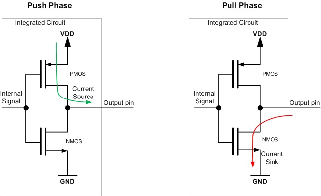 Fig. 1 Simplified schematic of a push-pull output
- Push phase – When the Internal Signal connected to the gates of the transistors (see the figure above) is set to a low logic level (logic 0), the PMOS transistor is activated and current flows through it from the VDD to the output pin. NMOS transistor is inactive (open) and not conducting.
- Pull phase – When the Internal Signal connected to the gates of the transistors is set to a high logic level (logic 1), the NMOS transistor is activated (closed) and current starts to flow through it from the output pin to the GND. At the same time, the PMOS transistor is inactive (open) and is not conducting current.
This type of output doesn’t allow connecting multiple devices together in a bus configuration, like the open drain output. Push-pull configuration is most commonly used in interfaces that have unidirectional lines (transmission on the line is only in a single direction – SPI, UART etc.).
As push-pull outputs are constantly driven (high or low), they provide better performance when it comes to the slopes of the generated output digital signals.
It should be noted that an output pin configured as push-pull can in most cases be dynamically reconfigured to become an input. This is achieved by closing both of the transistors, thus achieving high impedance state on the line. Then the line can be driven from other external devices and sensed with dedicated logic inside the integrated circuit.
Open Drain
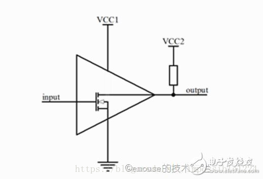
In open drain configuration, the logic behind the pin can drive it only to ground (logic 0). The other possible state is high impedance (Hi-Z). The implementation involves the use of a single transistor. If its drain terminal is open (the device is off) the pin is left floating to Hi-Z state. Driving it to high logic level requires the use of an additional circuit or component. In most cases, an external pull-up resistor is used (there are microcontrollers that provide internal pull-up resistors for open drain configurations).
On Fig. 2 we can see an open drain output. It is implemented using an N-channel MOS transistor that pulls the output pin to ground when the transistor is on and leaves it floating when the transistor is off.
 Fig. 2 Schematic of an open drain output
Open drain outputs are most commonly used in communication interfaces where multiple devices are connected on the same line (e.g I2C, One-Wire etc.). When all of the outputs of the devices connected to the line are in Hi-Z state, the line is driven to a default logic 1 level by a pull-up. Any device can pull the line to logic 0 using its open drain output and all devices can see this level.
There are few things that have to be considered when using a pull-up resistor with the open drain output configuration:
Rising edge slope – The pull-up resistor in combination with the inherent capacitance of the line forms a low-pass filter. Depending on the value of the resistor and the capacitance of the line there can be a visible difference in the slopes of the rising edges compared to the falling edges. The falling edge is sharper as it is achieved using the transistor which has very low internal resistance. The rising edge, however, is formed by the pull-up resistor and the aforementioned low-pass filtering effect is more pronounced.
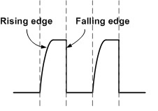 Fig. 1 Edges of square wave signal generated by an open drain output
Power consumption and noise interference – A trade-off exists when choosing the value of the pull-up resistors. When a device on the line drives logic 0 level, it will cause a higher current to flow through pull-up resistors with lower values and this will increase the power consumption. However, choosing higher valued resistors will, in turn, cause a lower current to flow through the resistor and this will make it easier for external interferences (noise) to be picked up on the line.
Summary
- Push-pull output is best suited for communication interfaces that have single direction lines (e.g SPI, UART etc.). Open drain is commonly used for bidirectional single line communication interfaces, where more than two devices are connected on the same line(e.g I2C, One-Wire etc.)
- Open drain output has higher power consumption during active transfers due to the pull-up resistors that are used.
- In general, the push-pull output has faster slopes than the open drain output.




【推荐】国内首个AI IDE,深度理解中文开发场景,立即下载体验Trae
【推荐】编程新体验,更懂你的AI,立即体验豆包MarsCode编程助手
【推荐】抖音旗下AI助手豆包,你的智能百科全书,全免费不限次数
【推荐】轻量又高性能的 SSH 工具 IShell:AI 加持,快人一步