Clock Gating
http://asic-soc.blogspot.com/2008/04/clock-gating.html
Clock Gating
2) Power consumed by flip-flops and
3) The power consumed by the clock buffer tree in the design.
It is good design idea to turn off the clock when it is not needed. Automatic clock gating is supported by modern EDA tools. They identify the circuits where clock gating can be inserted.
RTL clock gating works by identifying groups of flip-flops which share a common enable control signal. Traditional methodologies use this enable term to control the select on a multiplexer connected to the D port of the flip-flop or to control the clock enable pin on a flip-flop with clock enable capabilities. RTL clock gating uses this enable signal to control a clock gating circuit which is connected to the clock ports of all of the flip-flops with the common enable term. Therefore, if a bank of flip-flops which share a common enable term have RTL clock gating implemented, the flip-flops will consume zero dynamic power as long as this enable signal is false.
There are two types of clock gating styles available. They are:
1) Latch-based clock gating
2) Latch-free clock gating.
Latch free clock gating
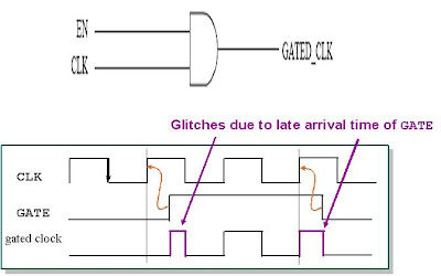
The latch-free clock gating style uses a simple AND or OR gate (depending on the edge on which flip-flops are triggered). Here if enable signal goes inactive in between the clock pulse or if it multiple times then gated clock output either can terminate prematurely or generate multiple clock pulses. This restriction makes the latch-free clock gating style inappropriate for our single-clock flip-flop based design.
Latch free clock gating
Latch based clock gating
The latch-based clock gating style adds a level-sensitive latch to the design to hold the enable signal from the active edge of the clock until the inactive edge of the clock. Since the latch captures the state of the enable signal and holds it until the complete clock pulse has been generated, the enable signal need only be stable around the rising edge of the clock, just as in the traditional ungated design style.
Latch based clock gating
Specific clock gating cells are required in library to be utilized by the synthesis tools. Availability of clock gating cells and automatic insertion by the EDA tools makes it simpler method of low power technique. Advantage of this method is that clock gating does not require modifications to RTL description.
References
[1] Frank Emnett and Mark Biegel, “Power Reduction Through RTL Clock Gating”, SNUG, San Jose, 2000
[2] PrimeTime User Guide
posted on 2010-09-01 19:24 Homography Matrix 阅读(2686) 评论(0) 编辑 收藏 举报


