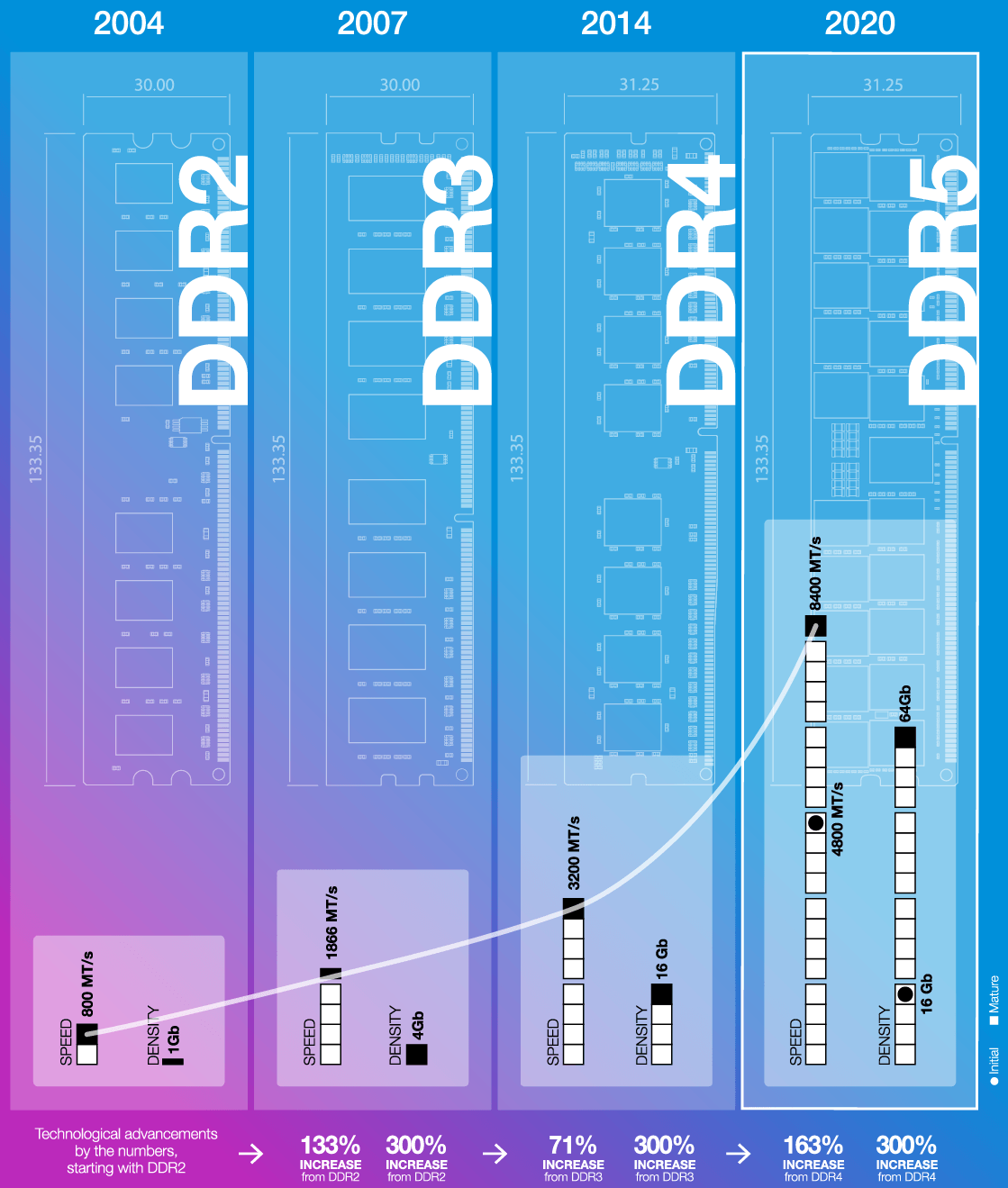
【收集+】DDR5 vs DDR4
Advantages of Migrating to DDR5
DDR5 is the next evolution in DRAM, bringing a robust list of new features geared to increase reliability, availability, and serviceability (RAS); reduce power; and dramatically improve performance. Some of the key feature differences between DDR4 and DDR5 are as follows:
| Feature/Option | DDR4 | DDR5 | DDR5 Advantage |
|---|---|---|---|
| Data rates | 1600-3200 MT/s | 3200-6400 MT/s | Increases performance and bandwidth |
| VDD/VDDQ/VPP | 1.2/1.2/2.5 V | 1.1/1.1/1.8 V | Lowers power |
| Internal VREF | VREFDQ | VREFDQ, VREFCA, VREFCS | Improves voltage margins, reduces BOM costs |
| Device densities | 2Gb-16Gb | 8Gb-64Gb | Enables larger monolithic devices |
| Prefetch | 8n | 16n | Keeps the internal core clock low |
| DQ receiver equalization | CTLE | DFE | Improves opening of the received DQ data eyes inside the DRAM |
| Duty cycle adjustment (DCA) | None | DQS and DQ | Improves signaling on the transmitted DQ/DQS pins |
| Internal DQS delay monitoring |
None | DQS interval oscillator | Increases robustness against environmental changes |
| On-die ECC | None | 128b+8b SEC, error check and scrub | Strengthens on-chip RAS |
| CRC | Write | Read/Write | Strengthens system RAS by protecting read data |
| Bank groups (BG)/banks | 4 BG x 4 banks (x4/x8) 2 BG x 4 banks (x16) |
8 BG x 2 banks (8Gb x4/x8) 4 BG x 2 banks (8Gb x16) 8 BG x 4 banks (16-64Gb x4/x8) 4 BG x 4 banks (16-64Gb x16) |
Improves bandwidth/performance |
| Command/address interface | ODT, CKE, ACT, RAS, CAS, WE, A<X:0> |
CA<13:0> |
Dramatically reduces the CA pin count |
| ODT | DQ, DQS, DM/DBI | DQ, DQS, DM, CA bus | Improves signal integrity, reduces BOM costs |
| Burst length | BL8 (and BL4) | BL16, BL32 (and BC8 OTF, BL32 OTF) |
Allows 64B cache line fetch with only 1 DIMM subchannel. |
| MIR (“mirror” pin) | None | Yes | Improves DIMM signaling |
| Bus inversion | Data bus inversion (DBI) | Command/address inversion (CAI) | Reduces VDDQ noise on modules |
| CA training, CS training | None | CA training, CS training | Improves timing margin on CA and CS pins |
| Write leveling training modes | Yes | Improved | Compensates for unmatched DQ-DQS path |
| Read training patterns | Possible with the MPR | Dedicated MRs for serial (userdefined), clock and LFSR -generated training patterns |
Makes read timing margin more robust |
| Mode registers | 7 x 17 bits | Up to 256 x 8 bits (LPDDR type read/write) |
Provides room to expand |
| PRECHARGE commands | All bank and per bank | All bank, per bank, and same bank | PREsb enables precharging-specific bank in each BG |
| REFRESH commands | All bank | All bank and same bank | REFsb enables refreshing of specific bank in each BG |
| Loopback mode | None | Yes | Enables testing of the DQ and DQS signaling |

【参考文献】
https://www.micron.com/products/dram/ddr5-sdram
-------
【信息收集,引用请声明出处,yvivid】https://www.cnblogs.com/yvivid/p/DDR5.html


 浙公网安备 33010602011771号