基于I.MX6UL平台的ADS1256驱动开发五.实现功能
在前面我们已经完成了基本的寄存器读写操作,下面我们就可以根据数据手册来完成基础AD功能的实现。
初始化
初始化的过程基本上是从AD板供应商提供的Demo移植的。
 1 void ADS1256_CfgADC(ADS1256_GAIN_E _gain, ADS1256_DRATE_E _drate)
 2 {
 3     g_tADS1256.Gain = _gain;
 4     g_tADS1256.DataRate = _drate;
 5
 6     ADS1256_WaitDRDY();
 7
 8     {
 9         uint8_t buf[4];        /* 暂存ADS1256 寄存器配置参数,之后连续写4个寄存器 */
10
11         /* 状态寄存器定义
12             Bits 7-4 ID3, ID2, ID1, ID0  Factory Programmed Identification Bits (Read Only)
13
14             Bit 3 ORDER: Data Output Bit Order
15                 0 = Most Significant Bit First (default)
16                 1 = Least Significant Bit First
17             Input data  is always shifted in most significant byte and bit first. Output data is always shifted out most significant
18             byte first. The ORDER bit only controls the bit order of the output data within the byte.
19
20             Bit 2 ACAL : Auto-Calibration
21                 0 = Auto-Calibration Disabled (default)
22                 1 = Auto-Calibration Enabled
23             When Auto-Calibration is enabled, self-calibration begins at the completion of the WREG command that changes
24             the PGA (bits 0-2 of ADCON register), DR (bits 7-0 in the DRATE register) or BUFEN (bit 1 in the STATUS register)
25             values.
26
27             Bit 1 BUFEN: Analog Input Buffer Enable
28                 0 = Buffer Disabled (default)
29                 1 = Buffer Enabled
30
31             Bit 0 DRDY :  Data Ready (Read Only)
32                 This bit duplicates the state of the DRDY pin.
33
34             ACAL=1使能自校准功能。当 PGA,BUFEEN, DRATE改变时会启动自校准
35         */
36         buf[0] = (0 << 3) | (1 << 2) | (0 << 1);//此处(0 << 1)表示关闭BUFFER,改为(1 << 1)表示打开BUFFER
37         /*
38         打开或关闭BUFFER会影响芯片可采集电压范围.详见ADS1256数据手册第3页
39         关闭BUFFER,采集范围:AGND-0.1    ~    AVDD+0.1
40         打开BUFFER,采集范围:AGND            ~    AVDD+2.0
41         */
42
43         buf[1] = 0x08;    /* 高四位0表示AINP接 AIN0,  低四位8表示 AINN 固定接 AINCOM */
44
45         /*    ADCON: A/D Control Register (Address 02h)
46             Bit 7 Reserved, always 0 (Read Only)
47             Bits 6-5 CLK1, CLK0 : D0/CLKOUT Clock Out Rate Setting
48                 00 = Clock Out OFF
49                 01 = Clock Out Frequency = fCLKIN (default)
50                 10 = Clock Out Frequency = fCLKIN/2
51                 11 = Clock Out Frequency = fCLKIN/4
52                 When not using CLKOUT, it is recommended that it be turned off. These bits can only be reset using the RESET pin.
53
54             Bits 4-2 SDCS1, SCDS0: Sensor Detect Current Sources
55                 00 = Sensor Detect OFF (default)
56                 01 = Sensor Detect Current = 0.5 μ A
57                 10 = Sensor Detect Current = 2 μ A
58                 11 = Sensor Detect Current = 10μ A
59                 The Sensor Detect Current Sources can be activated to verify  the integrity of an external sensor supplying a signal to the
60                 ADS1255/6. A shorted sensor produces a very small signal while an open-circuit sensor produces a very large signal.
61
62             Bits 2-0 PGA2, PGA1, PGA0: Programmable Gain Amplifier Setting
63                 000 = 1 (default)
64                 001 = 2
65                 010 = 4
66                 011 = 8
67                 100 = 16
68                 101 = 32
69                 110 = 64
70                 111 = 64
71         */
72         buf[2] = (0 << 5) | (0 << 3) | (_gain << 0);
73         //ADS1256_WriteReg(REG_ADCON, (0 << 5) | (0 << 2) | (GAIN_1 << 0));    /* 选择1;1增益, 输入正负5V */
74
75         /* 因为切换通道和读数据耗时 123uS, 因此扫描中断模式工作时,最大速率 = DRATE_1000SPS */
76         buf[3] = s_tabDataRate[_drate];    // DRATE_10SPS;    /* 选择数据输出速率 */
77
78         CS_0();    /* SPI片选 = 0 */
79         ADS1256_Send8Bit(CMD_WREG | 0);    /* 写寄存器的命令, 并发送寄存器地址 */
80         ADS1256_Send8Bit(0x03);            /* 寄存器个数 - 1, 此处3表示写4个寄存器 */
81
82         ADS1256_Send8Bit(buf[0]);    /* 设置状态寄存器 */
83         ADS1256_Send8Bit(buf[1]);    /* 设置输入通道参数 */
84         ADS1256_Send8Bit(buf[2]);    /* 设置ADCON控制寄存器,增益 */
85         ADS1256_Send8Bit(buf[3]);    /* 设置输出数据速率 */
86
87         CS_1();    /* SPI片选 = 1 */
88     }
初始化主要就是对STATUS、MUX、ADCON和DRATE4个寄存器进行配置。配置的思路备注里很清楚了。
读取数据
读取数据要切换通道,通道的切换是通过设置MUX寄存器实现的,但是MUX寄存器在写入后需要给其他的指令才可以读取数据,手册上有相关的时序图
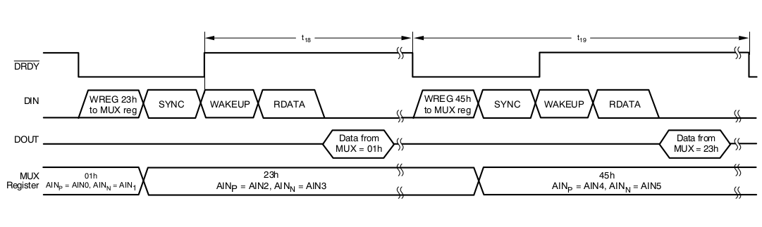
我们只需要在DRDY被拉低的时候配置MUX寄存器就行了,要注意点是RDATA指令读取到的数据时上一组MUX选择的输入信号。按照上面的时序图,DRDY拉低以后配置的MUX选择的是2、3脚输入的信号,但是读取到的数据是MUX=0x01时的数据。待下个读取周期读取到的数据则是MUX=0x23时候的。
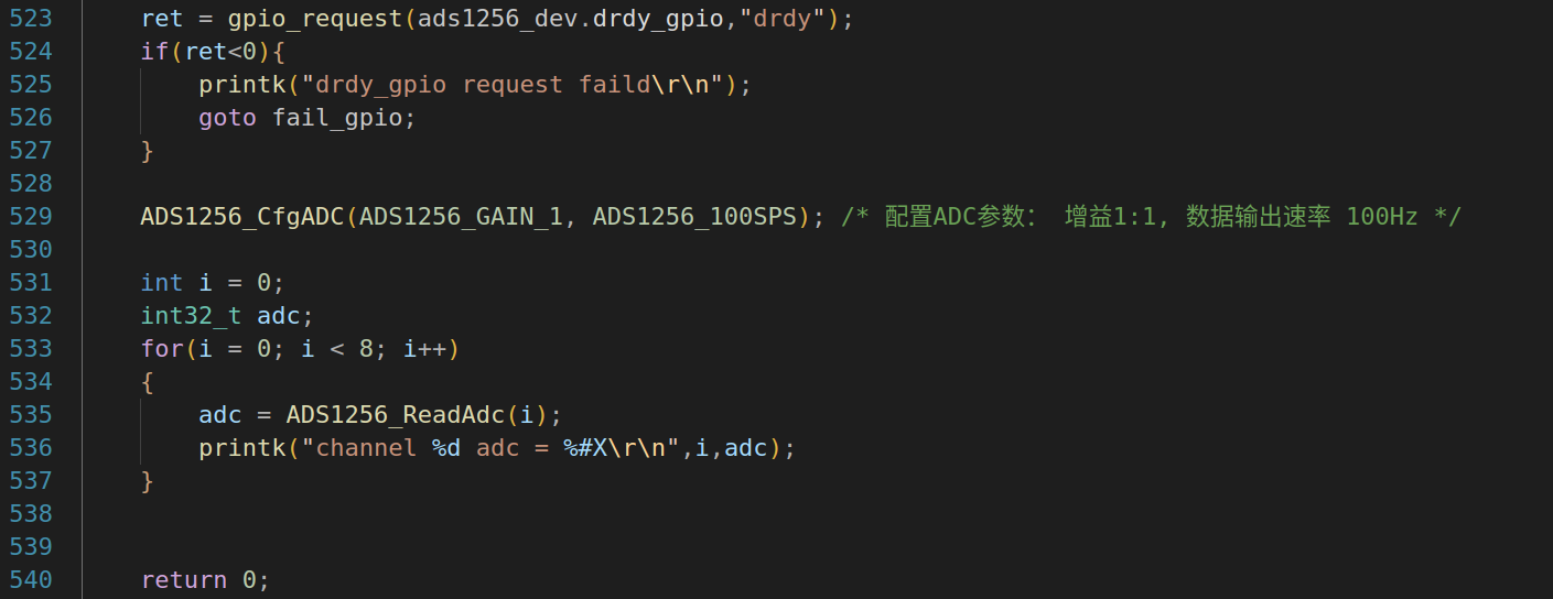
 1 /**
 2  * @brief 读取指定通道码值
 3  *
 4  * @param _ch
 5  * @return int32_t
 6  */
 7 int32_t ADS1256_ReadAdc(uint8_t _ch)
 8 {
 9
10     // while (DRDY_IS_LOW());
11
12     /* ADS1256 数据手册第21页 */
13     ADS1256_WaitDRDY();        /* 等待 DRDY = 0 */
14
15     ADS1256_SetChannal(_ch);    /* 切换模拟通道 */
16     udelay(5);
17
18     ADS1256_WriteCmd(CMD_SYNC);
19     udelay(5);
20
21     ADS1256_WriteCmd(CMD_WAKEUP);
22     udelay(5);
23
24     return (int32_t)ADS1256_ReadData();
25 }
前面一章结尾说了,我们这一版本的驱动不用中断来触发采样,所以做了个延时来轮询DRDY的状态,只要DRDY变低,就开始切换通道,发送同步指令(SYNC),唤醒指令(WAKEUP),最后是读取指令。完成以后,我们可以测试一下
加载看看效果
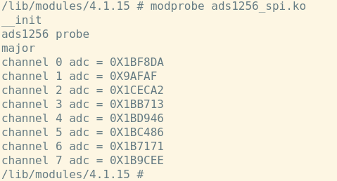
到此为止,我们已经拿到AD转换的码值了。
用户态的交互
现在我们已经在内核中实现了模块的驱动,但是我们需要在用户态的程序中获取到实际的数据,并且由于在内核中最好不要处理浮点类数据,我们在文件操作合集中的对应函数中将数据传递给用户态程序
 1 ssize_t ads1256_read(struct file *file, char __user *buf, size_t cnt, loff_t *off)
 2 {
 3
 4     struct ads1256_device *dev = (struct ads1256_device *)file->private_data;
 5     int ret = 0;
 6     uint8_t ch_num=8;
 7     int32_t adc[8];
 8     int i;
 9
10     printk("ads1256 read\r\n");
11     for (i = 0; i < ch_num; i++)                            //数据提取与转换
12     {
13         /* 从全局缓冲区读取采样结果。 采样结果是在中断服务程序中读取的。*/
14         adc[i] = ADS1256_ReadAdc(i);
15     }
16     ret = copy_to_user(buf,adc,sizeof(adc));
17     return ret;
18 }
就是在一个8次的for循环中,分别读取各个通道的AD码值,然后通过copy_to_user传递给用户态就可以了。
用户态程序
这里只体现如何从内核态拿到数据并且如何从码值换算到对应的电压值上
 1 #include <sys/types.h>
 2 #include <sys/stat.h>
 3 #include <fcntl.h>
 4 #include <unistd.h>
 5 #include <stdio.h>
 6 #include <stdlib.h>
 7
 8
 9 /**
10  * @brief
11  *
12  * @param argc                      //参数个数
13  * @param argv                      //参数
14  * @return int
15  */
16 int main(int argc,char *argv[])
17 {
18     char *filename;                 //文件名
19
20     int value = 0;
21     int32_t adc[8];
22     float volt[8];
23     int ret = 0;                    //初始化操作返回值
24     int f = 0;                      //初始化文件句柄
25     int i = 0;
26
27     filename = argv[1];
28     if(argc != 2){                  //输入参数个数不为3,提示输入格式错误
29         printf("input format error!\r\n");
30     }
31     printf("filename: %s\r\n", filename);
32
33     f = open(filename, O_RDWR);     //打开文件
34
35     if(f < 0){
36     printf("file open error\r\n");
37     return -1;
38     }
39
40     read(f,&adc,sizeof(adc));
41
42     for(i=0;i<8;i++){
43         volt[i] = (float)adc[i] / 8388607 *5.0;
44         printf("channel %d volt = %.5f\r\n",i,volt[i]);
45     }
46
47     close(f);                       //关闭文件
48     return 0;
49 }
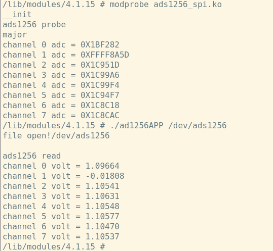
这里偷了个懒,不考虑负电压的情况,直接将码值换算至对应的电压上。由于我们在配置IC的时候将PGA配置为默认值1,所以输入量程为±5V,在最高位为0的时候为正电压值,5V对应码值为0x7FFFFF,对应值为1/8388607。乘以5就是每个LSB对应的电压值。在编译的时候可以加上下面加红的命令来指定一下指令集,使能硬件浮点运算
arm-linux-gnueabihf-gcc -march=armv7-a -mfpu=neon -mfloat-abi=hard ad1256APP.c -o ad1256APP
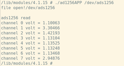
搞定以后可以测试一下
因为项目还用不到负电压的测量,这里先不考虑负电压的计算方式。并且还可以根据实际码值来动态调整PGA的值,都是可以后期优化的。先这样吧!
存在BUG
从开发板上引了个3.3V的信号,加载AIN1上时候CHANNEL1是有反应的
理论上应该是channel0有输出的。应该是MUX设置的时候有问题。留着回来改一下!