Address Space and Address Translation
Physical Address Space
In protected mode, the IA-32 architecture provides a normal physical address space of 4 GBytes (232
bytes). This is the address space that the processor can address on its address bus. This address space is flat (unsegmented), with addresses ranging continuously from 0 to FFFFFFFFH. This physical address space can be mapped to read-write memory, read-only memory, and memory mapped I/O. The memory mapping facilities described in this chapter can be used to divide this physical memory up into segments and/or pages.
Starting with the Pentium Pro processor, the IA-32 architecture also supports an extension of the physical address space to 2 to 36 bytes (64 GBytes); with a maximum physical address of FFFFFFFFFH. This extension is invoked in either of two ways:
• Using the physical address extension (PAE) flag, located in bit 5 of control register CR4.
• Using the 36-bit page size extension (PSE-36) feature (introduced in the Pentium III processors).
Physical address support has since been extended beyond 36 bits. See Chapter 4, “Paging” for more information about 36-bit physical addressing.
Intel® 64 Processors and Physical Address Space
On processors that support Intel 64 architecture (CPUID.80000001H:EDX[29] = 1), the size of the physical
address range is implementation-specific and indicated by CPUID.80000008H:EAX[bits 7-0].
For the format of information returned in EAX, see “CPUID—CPU Identification” in Chapter 3 of the Intel® 64 and IA-32 Architectures Software Developer’s Manual, Volume 2A. See also: Chapter 4, “Paging.”
Logical And Linear Addresses
At the system-architecture level in protected mode, the processor uses two stages of address translation to arrive at a physical address: logical-address translation and linear address space paging.
Even with the minimum use of segments, every byte in the processor’s address space is accessed with a logical
address.
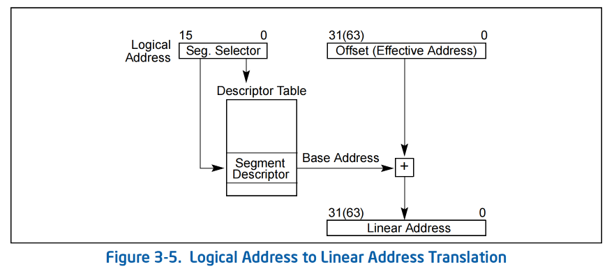
A logical address consists of a 16-bit segment selector and a 32-bit offset (see Figure 3-5). The segment selector identifies the segment the byte is located in and the offset specifies the location of the byte in the segment relative to the base address of the segment.
The processor translates every logical address into a linear address. A linear address is a 32-bit address in the
processor’s linear address space. Like the physical address space, the linear address space is a flat (unsegmented), 2 to 32-byte address space, with addresses ranging from 0 to FFFFFFFFH. The linear address space contains all the segments and system tables defined for a system.
To translate a logical address into a linear address, the processor does the following:
1. Uses the offset in the segment selector to locate the segment descriptor for the segment in the GDT or LDT and reads it into the processor. (This step is needed only when a new segment selector is loaded into a segment
register.)
2. Examines the segment descriptor to check the access rights and range of the segment to ensure that the
segment is accessible and that the offset is within the limits of the segment.
3. Adds the base address of the segment from the segment descriptor to the offset to form a linear address.
If paging is not used, the processor maps the linear address directly to a physical address (that is, the linear
address goes out on the processor’s address bus). If the linear address space is paged, a second level of address translation is used to translate the linear address into a physical address.

Logical Address Translation in IA-32e Mode
In IA-32e mode, an Intel 64 processor uses the steps described above to translate a logical address to a linear
address. In 64-bit mode, the offset and base address of the segment are 64-bits instead of 32 bits. The linear address format is also 64 bits wide and is subject to the canonical form requirement.
Each code segment descriptor provides an L bit. This bit allows a code segment to execute 64-bit code or legacy 32-bit code by code segment.
Segment Selectors
A segment selector is a 16-bit identifier for a segment (see Figure 3-6). It does not point directly to the segment, but instead points to the segment descriptor that defines the segment. A segment selector contains the following items:
Index
(Bits 3 through 15) — Selects one of 8192 descriptors in the GDT or LDT. The processor multiplies
the index value by 8 (the number of bytes in a segment descriptor) and adds the result to the base
address of the GDT or LDT (from the GDTR or LDTR register, respectively).
TI (table indicator) flag
(Bit 2) — Specifies the descriptor table to use: clearing this flag selects the GDT; setting this flag
selects the current LDT.
Requested Privilege Level (RPL)
(Bits 0 and 1) — Specifies the privilege level of the selector. The privilege level can range from 0 to
3, with 0 being the most privileged level. See Section 5.5, “Privilege Levels”, for a description of the
relationship of the RPL to the CPL of the executing program (or task) and the descriptor privilege
level (DPL) of the descriptor the segment selector points to.
The first entry of the GDT is not used by the processor. A segment selector that points to this entry of the GDT (that is, a segment selector with an index of 0 and the TI flag set to 0) is used as a “null segment selector.” The processor does not generate an exception when a segment register (other than the CS or SS registers) is loaded with a null selector. It does, however, generate an exception when a segment register holding a null selector is used to access memory. A null selector can be used to initialize unused segment registers. Loading the CS or SS register with a null segment selector causes a general-protection exception (#GP) to be generated.
Segment selectors are visible to application programs as part of a pointer variable, but the values of selectors are usually assigned or modified by link editors or linking loaders, not application programs.

Segment Registers
To reduce address translation time and coding complexity, the processor provides registers for holding up to 6
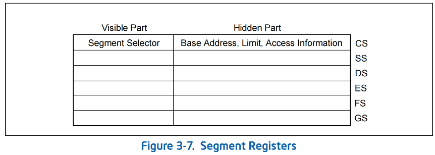
segment selectors (see Figure 3-7). Each of these segment registers support a specific kind of memory reference (code, stack, or data). For virtually any kind of program execution to take place, at least the code-segment (CS), data-segment (DS), and stack-segment (SS) registers must be loaded with valid segment selectors. The processor also provides three additional data-segment registers (ES, FS, and GS), which can be used to make additional data segments available to the currently executing program (or task).
For a program to access a segment, the segment selector for the segment must have been loaded in one of the
segment registers. So, although a system can define thousands of segments, only 6 can be available for immediate use. Other segments can be made available by loading their segment selectors into these registers during program execution.

Every segment register has a “visible” part and a “hidden” part. (The hidden part is sometimes referred to as a
“descriptor cache” or a “shadow register.”) When a segment selector is loaded into the visible part of a segment register, the processor also loads the hidden part of the segment register with the base address, segment limit, and access control information from the segment descriptor pointed to by the segment selector. The information cached in the segment register (visible and hidden) allows the processor to translate addresses without taking extra bus cycles to read the base address and limit from the segment descriptor. In systems in which multiple processors have access to the same descriptor tables, it is the responsibility of software to reload the segment registers when the descriptor tables are modified. If this is not done, an old segment descriptor cached in a segment register might be used after its memory-resident version has been modified.
Two kinds of load instructions are provided for loading the segment registers:
1. Direct load instructions such as the MOV, POP, LDS, LES, LSS, LGS, and LFS instructions. These instructions
explicitly reference the segment registers.
2. Implied load instructions such as the far pointer versions of the CALL, JMP, and RET instructions, the SYSENTER and SYSEXIT instructions, and the IRET, INT n, INTO, INT3, and INT1 instructions. These instructions change the contents of the CS register (and sometimes other segment registers) as an incidental part of their
operation.
The MOV instruction can also be used to store the visible part of a segment register in a general-purpose register.
Segment Loading Instructions in IA-32e Mode
Because ES, DS, SS segment registers are not used in 64-bit mode, their fields (base, limit, and attribute) in segment descriptor registers are ignored. Some forms of segment load instructions are also invalid (for example, LDS, POP ES). Address calculations that reference the ES, DS, or SS segments are treated as if the segment base is zero.
The processor checks that all linear-address references are in canonical form instead of performing limit checks. Mode switching does not change the contents of the segment registers or the associated descriptor registers. These registers are also not changed during 64-bit mode execution, unless explicit segment loads are performed.
In order to set up compatibility mode for an application, segment-load instructions (MOV to Sreg, POP Sreg) work normally in 64-bit mode. An entry is read from the system descriptor table (GDT or LDT) and is loaded in the hidden portion of the segment register. The descriptor-register base, limit, and attribute fields are all loaded. However, the contents of the data and stack segment selector and the descriptor registers are ignored.
When FS and GS segment overrides are used in 64-bit mode, their respective base addresses are used in the linear address calculation: (FS or GS).base + index + displacement. FS.base and GS.base are then expanded to the full linear-address size supported by the implementation. The resulting effective address calculation can wrap across positive and negative addresses; the resulting linear address must be canonical.
In 64-bit mode, memory accesses using FS-segment and GS-segment overrides are not checked for a runtime limit nor subjected to attribute-checking. Normal segment loads (MOV to Sreg and POP Sreg) into FS and GS load a standard 32-bit base value in the hidden portion of the segment register. The base address bits above the standard 32 bits are cleared to 0 to allow consistency for implementations that use less than 64 bits.
The hidden descriptor register fields for FS.base and GS.base are physically mapped to MSRs in order to load all address bits supported by a 64-bit implementation. Software with CPL = 0 (privileged software) can load all
supported linear-address bits into FS.base or GS.base using WRMSR. Addresses written into the 64-bit FS.base and GS.base registers must be in canonical form. A WRMSR instruction that attempts to write a non-canonical address to those registers causes a #GP fault.
When in compatibility mode, FS and GS overrides operate as defined by 32-bit mode behavior regardless of the
value loaded into the upper 32 linear-address bits of the hidden descriptor register base field. Compatibility mode ignores the upper 32 bits when calculating an effective address.
A new 64-bit mode instruction, SWAPGS, can be used to load GS base. SWAPGS exchanges the kernel data structure pointer from the IA32_KERNEL_GS_BASE MSR with the GS base register. The kernel can then use the GS prefix on normal memory references to access the kernel data structures. An attempt to write a non-canonical value (using WRMSR) to the IA32_KERNEL_GS_BASE MSR causes a #GP fault.


 浙公网安备 33010602011771号