app_intf笔记
pg150-ultrascale-memory-ip.pdf
Protocol Description
User Interface
| Signal | I/O | Description |
|---|---|---|
| app_addr[APP_ADDR_WIDTH – 1:0] | I | 地址线. |
| app_cmd[2:0] | I | 命令,写为3'b000;读为3'b001. |
| app_en | I | 命令通道使能 |
| app_rdy | O | 命令通道ready |
| app_rd_data [APP_DATA_WIDTH – 1:0] | O | 读数据 |
| app_rd_data_end | O | 指示最后一笔读数据 |
| app_rd_data_valid | O | 读数据有效信号 |
| app_wdf_data [APP_DATA_WIDTH – 1:0] | I | 写数据 |
| app_wdf_end | I | 指示最后一笔写数据 |
| app_wdf_mask [APP_MASK_WIDTH – 1:0] | I | 写数据mask |
| app_wdf_rdy | O | 写数据通道ready |
| app_wdf_wren | I | 写数据通道使能 |
| ui_clk | O | app接口时钟 |
| init_calib_complete | O | 初始化完信号 |
| ui_clk_sync_rst | O | app接口复位,高有效 |
app_addr[APP_ADDR_WIDTH – 1:0]
app_addr受参数MEM_ADDR_ORDER影响
ROW_BANK_COLUMN
| SDRAM | app_addr Mapping |
|---|---|
| Rank | (RANK == 1) ? 1'b0: |
| Row | app_addr[COL_WIDTH + BANK_WIDTH +: ROW_WIDTH] |
| Column | app_addr[0 +: COL_WIDTH] |
| Bank | app_addr[COL_WIDTH +: BANK_WIDTH] |
BANK_ROW_COLUMN
| SDRAM | app_addr Mapping |
|---|---|
| Rank | (RANK == 1) ? 1'b0: |
| Row | app_addr[COL_WIDTH +: ROW_WIDTH] |
| Column | app_addr[0 +: COL_WIDTH] |
| Bank | app_addr[COL_WIDTH + ROW_WIDTH +: BANK_WIDTH] |
app_cmd[2:0]
Commands for app_cmd[2:0]
| Operation | app_cmd[2:0] Code |
|---|---|
| Write | 000 |
| Read | 001 |
app_en
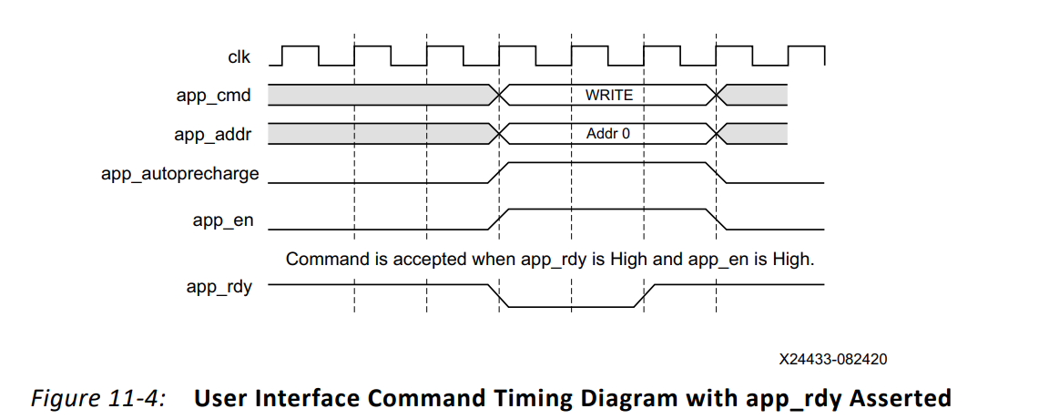
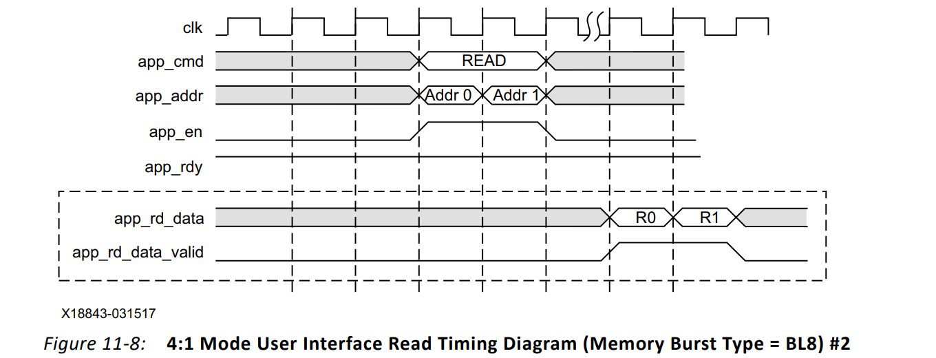
This input strobes in a request. Apply the desired values to app_addr[], app_cmd[2:0], and app_hi_pri, and then assert app_en to submit the request to the user interface. This initiates a handshake that the user interface acknowledges by asserting app_rdy.
app_hi_pri
This input indicates that the current request is a high priority
app_wdf_data[APP_DATA_WIDTH – 1:0]
This bus provides the data currently being written to the external memory.
app_wdf_end
This input indicates that the data on the app_wdf_data[] bus in the current cycle is the last data for the current request.
app_wdf_mask[APP_MASK_WIDTH – 1:0]
This bus indicates which bits of app_wdf_data[] are written to the external memory and which bits remain in their current state. The bytes are masked by setting a value of 1 to the corresponding bits in app_wdf_mask. For example, if the application data width is 256, the mask width takes a value of 32. The least significant byte [7:0] of app_wdf_data is masked using Bit[0] of app_wdf_mask and the most significant byte [255:248] of app_wdf_data is masked using Bit[31] of app_wdf_mask. Hence if you have to mask the last DWORD, that is, bytes 0, 1, 2, and 3 of app_wdf_data, the app_wdf_mask should be set to 32'h0000_000F.
app_wdf_wren
This input indicates that the data on the app_wdf_data[] bus is valid.
app_rdy
This output indicates whether the request currently being submitted to the user interface is accepted. If the user interface does not assert this signal after app_en is asserted, the current request must be retried. The app_rdy output is not asserted if:
° PHY/Memory initialization is not yet completed.
° All the bank machines are occupied (can be viewed as the command buffer being full).
- A read is requested and the read buffer is full.
- A write is requested and no write buffer pointers are available.
° A periodic read is being inserted.
app_rd_data[APP_DATA_WIDTH – 1:0]
This output contains the data read from the external memory.
app_rd_data_end
This output indicates that the data on the app_rd_data[] bus in the current cycle is the last data for the current request.
app_rd_data_valid
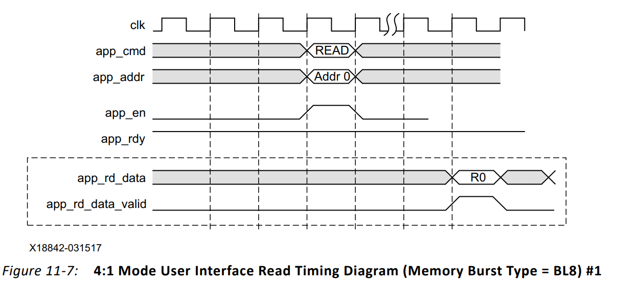
This output indicates that the data on the app_rd_data[] bus is valid.
app_wdf_rdy
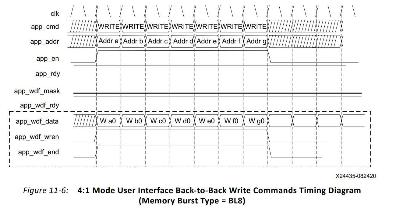
This output indicates that the write data FIFO is ready to receive data. Write data is accepted when both app_wdf_rdy and app_wdf_wren are asserted.
ui_clk_sync_rst
This is the reset from the user interface which is in synchronous with ui_clk.
ui_clk
This is the output clock from the user interface. It must be a quarter the frequency of the clock going out to the external SDRAM, which depends on 2:1 or 4:1 mode selected in Vivado IDE.
init_calib_complete
PHY asserts init_calib_complete when calibration is finished. The application has no need to wait for init_calib_complete before sending commands to the Memory Controller.
Command Path
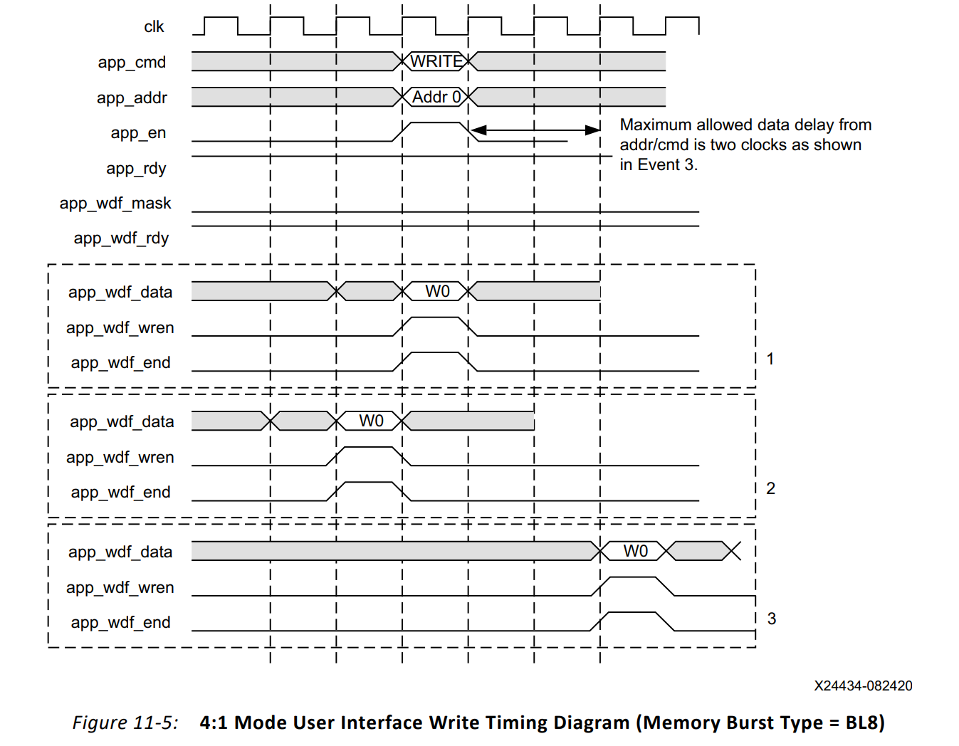
A non back-to-back write command can be issued as shown in Figure 11-5. This figure depicts three scenarios for the app_wdf_data, app_wdf_wren, and app_wdf_end signals as follows: 1. Write data is presented along with the corresponding write command. 2. Write data is presented before the corresponding write command. 3. Write data is presented after the corresponding write command, but should not exceed the limitation of two clock cycles. For write data that is output after the write command has been registered, as shown in Note 3 (Figure 11-5), the maximum delay is two clock cycles.
Write Path
Read Path

 浙公网安备 33010602011771号