ARM-CortexA72微架构
介绍
ARM announced the Cortex-A72, the high-end successor to the Cortex-A57, near the beginning of 2015. For more than a year now, SoC vendors have been working on integrating the new CPU core into their products. Now that mobile devices using the A72 are imminent, it’s a good time to discuss what makes ARM’s flagship CPU tick.
With the A57, ARM looked to expand the market for its CPUs beyond mobile devices and into the low-power server market. Using a single CPU architecture for both smartphones and servers sounds unreasonable, but according to ARM’s Mike Filippo, lead architect for the A72, high-end mobile workloads put a lot of pressure on caches, branch prediction, and the translation lookaside buffer (TLB), which are also important for server workloads. Where the A57 seemed skewed towards server applications based on its power consumption, the A72 takes a more balanced approach and looks to be a better fit for mobile.
The Cortex-A72 is an evolution of the Cortex-A57; the baseline architecture is very similar. However, ARM tweaked the entire pipeline for better power and performance. Perhaps the A57’s biggest weakness was its relatively high power consumption, especially on the 20nm node, which severely limited sustained performance in mobile devices, relegating it to short, bursty workloads and forcing SoCs to use the lower-performing Cortex-A53 cores for extended use.
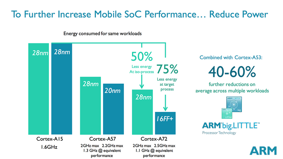
ARM looks to correct this issue with the A72, going back and optimizing nearly every one of the A57’s logical blocks to reduce power consumption. For example, ARM was able to realize a 35-40% reduction in dynamic power for the decoder stage, and by using an early IC tag lookup, the A72’s 3-way L1 instruction and 2-way L1 data caches also use less power, similar to what direct-mapped caches would use. According to ARM, all of the changes made to the A72 result in about a 15% reduction in energy use compared to the A57 when both cores are running the same workload at the same frequency and using the same 28nm process. The A72 sees an even more significant reduction when using a modern FinFET process, such as TSMC’s 16nm FinFET+, where an A72 core stays within a 750mW power envelope at 2.5GHz, according to ARM.
架构概述
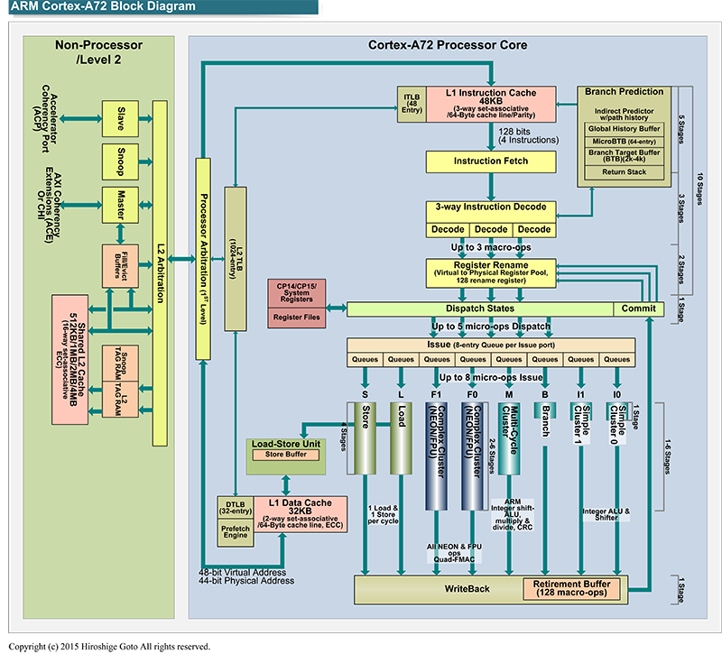
取指
The A72 sees improvements to performance too, starting with a much improved branch prediction algorithm. ARM’s performance modeling group is continuously updating the simulated workloads fed to the processor, and these affect the design of the branch predictor as well as the rest of the CPU. For example, based on these workloads, ARM found that instruction offsets between branches are often close together in memory. This allowed it to make certain optimizations to its dynamic predictor, like enabling the Branch Target Buffer (BTB) to hold anywhere from 2000 large branches to 4000 small branches.
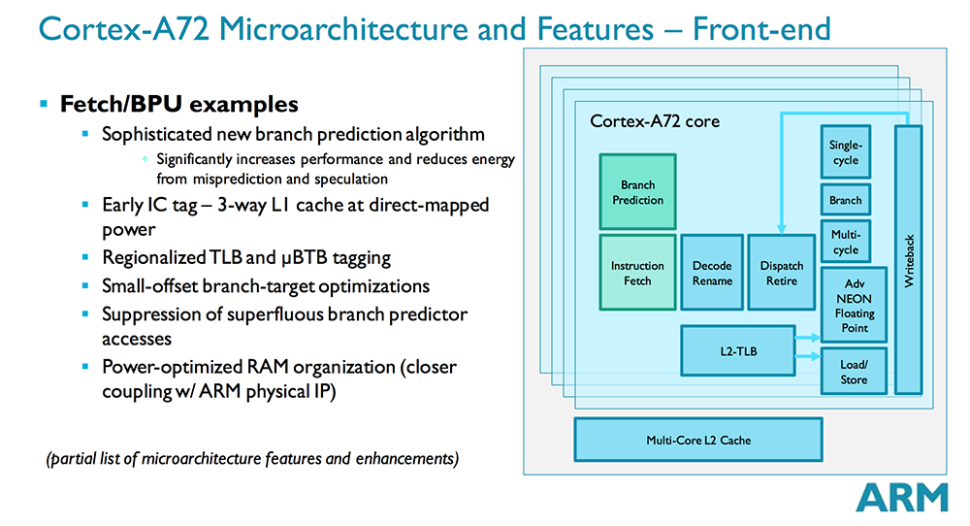
Because real-world code tends to include many branch instructions, branch prediction and speculative execution can greatly improve performance—something that’s usually not tested by synthetic benchmarks. Better branch prediction usually costs more power, however, at least in the front-end. This is at least partially offset by fewer mispredictions, saving power on the back-end by avoiding pipeline flushes and wasted clock cycles. Another way ARM is saving power is by shutting off the branch predictor in situations where it’s unnecessary. There are many blocks, for instance, where instructions between branches are greater than the 16-byte instruction window the predictor uses, so it makes sense to shut it down because the predictor will obviously not hit a branch in that section of code.
解码/重命名
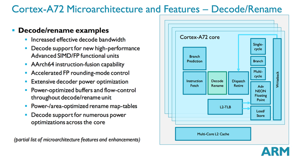
The rest of the front-end is still in-order with a 3-way decoder just like the A57. However, unlike the A57’s decoder, which decodes instructions into micro-ops, the A72 decodes instructions into macro-ops that can contain multiple micro-ops. It also supports AArch64 instruction-fusion within the decoder. These macro-ops get “late-cracked” into multiple micro-ops at the dispatch level, which is now capable of issuing up to five micro-ops, up from three on the A57. ARM quotes a 1.08 micro-ops per instruction ratio on average when executing common code. Improving the A72’s front-end bandwidth helps keep the new lower-latency execution units fed and also reduces the number of cases where the front-end bottlenecks performance.
分发/退休
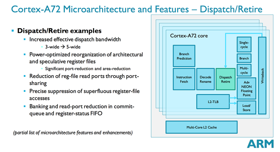
As explained above, the A72 is now able to dispatch five micro-ops into the issue queues that feed the execution units. The issue queues still hold a total of 66 micro-ops like they did on the A57—eight entries for each pipeline except the branch execution unit queue that holds ten entries. While queue depth is the same, the A72 does have an improved issue-queue load-balancing algorithm that eliminates some additional cases of mismatched utilization of the FP/Advanced SIMD units.
The A72’s dispatch unit also sees significant area and power reductions by reorganizing the architectural and speculative register files. ARM also reduced the number of register read ports through port sharing. This is important because the read ports are very sensitive to timing and require larger gates to enable higher core frequencies, which causes a second-order effect to area and power by pushing other components further away. In total, the dispatch unit sees a 10% reduction in area with no adverse affect on performance.
执行单元
Moving to the out-of-order back-end, the A72 can still issue eight micro-ops per cycle like the A57, but execution latency is significantly reduced because of the next-generation FP/Advanced SIMD units. Floating-point instructions see up to a 40% latency reduction over the A57 (5-cycle to 3-cycle FMUL), and the new Radix-16 FP divider doubles bandwidth. The changes to the integer units are less extensive, but they also make the change to a Radix-16 integer divider (doubling bandwidth over A57) and a 1-cycle CRC unit.
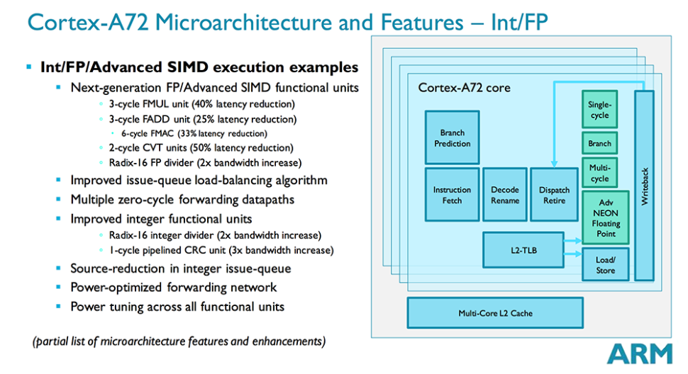
Reducing pipeline length improves performance directly by reducing latency and indirectly by easing pressure on the out-of-order window. So even though the instruction reorder buffer remains at 128 entries like the A57, it now has more opportunity to extract instruction-level parallelism (ILP).
Expanded zero-cycle forwarding (all integer and some floating-point instructions) further reduces execution latency. This technique allows dependent operations—where the output of one instruction is the input to the next—to directly follow each other in the pipeline without a one or more cycle wait period between them. This is an important optimization for cryptography.
存取
The load/store unit also sees improvements to both performance and power. One of the big changes from A57 is a move away from separate L1 and L2 prefetchers to a more sophisticated combined prefetcher that fetches from both the L1 and L2 caches. This improves bandwidth while also reducing power. There are additional power optimizations to the L1-hit pipeline and forwarding network too.
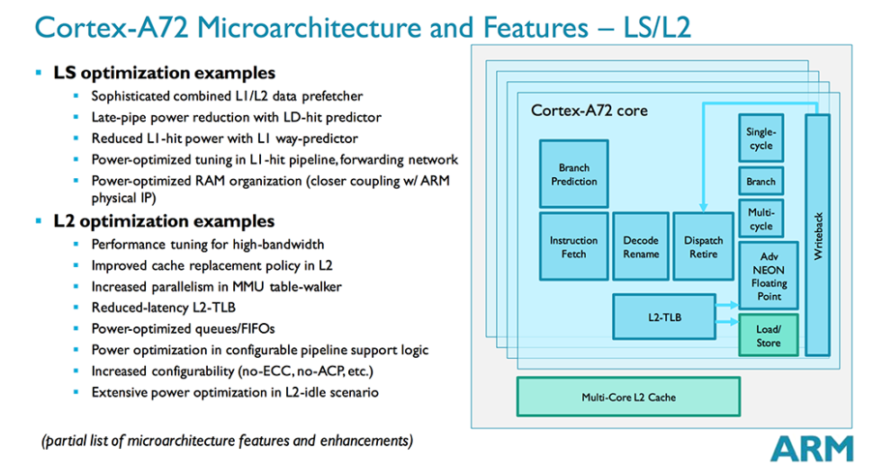
The L2 cache sees significant optimizations for higher bandwidth workloads. Memory streaming tasks see the biggest benefit, but ARM says general floating-point and integer workloads also see an increase in performance. A new cache replacement policy increases hit rates in the L2, which again improves performance and reduces power overall.
Another optimization increases parallelism in the table-walker hardware for the memory management unit (MMU), responsible for translating virtual memory addresses to physical addresses among other things. Together with a lower-latency L2 TLB, performance improves for programs that spread data across several data pages such as Web browsers.
最后的思考
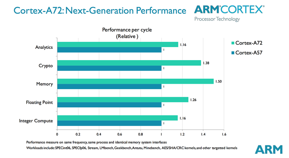
At a high-level, the A72 looks nearly identical to the A57, but at a lower level there are a significant number of changes throughout the entire pipeline that appear to make the A72 a decent upgrade. The most notable changes affecting performance are the improved branch prediction, increased dispatch bandwidth, lower-latency execution units, and higher bandwidth L2 cache. All of these enhancements, and many more which we did not discuss here, lead to better performance—between 16-50% across a range of synthetic benchmarks, according to ARM. Real-world performance gains will be less, of course, but A72 is definitely an improvement over the A57, especially with floating-point workloads.
The A72 is not a pure performance play, however. ARM is targeting a much higher power efficiency with this architecture than with any previous high-end CPU core. It’s clear from the lengthy list of optimizations discussed above that reducing power consumption was paramount; many of the changes are purely focused on power with no net performance gain.
Reducing power and area—the A72 achieves a 10% core area reduction overall—obviously has a positive effect on battery life and cost, but it has a secondary effect on performance too. Normally, reducing latency in the execution units puts pressure on the max attainable core frequency due to increased circuit complexity and tighter timing windows; however, the A72’s power and area optimizations elsewhere, not to mention the move to FinFET, actually allow the A72 to reach a slightly higher frequency. Reducing power also reduces thermal load, allowing for higher sustained performance, something the A57 struggles with at 20nm.
The Cortex-A72 may not be a revolutionary design that catapults it above Apple’s Twister CPU in the A9 SoC for single-core performance or undercuts the A53 in power consumption, but it’s a significant update nonetheless, addressing the A57’s issues by enabling higher peak and sustained performance while using less power.

 浙公网安备 33010602011771号