
Paper5 MOSFET-工程调试经验
振铃问题
1. 振铃的定义
2. 降低振铃的方法
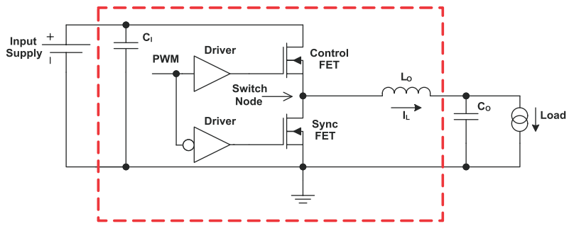
- Minimize the node length between the positive terminal of the input capacitors and the Drain pin of the Control FET.
- Minimize the node length between the negative terminal of the input capacitors and the Source pin of the Sync FET.
- ceramic input capacitors were used due to the inherently low equivalent series inductance (ESL)
- the placement of the driver IC to be put directly below the power MOSFETs on the bottom layer. This minimizes the distance of gate drive traces.
3. 振铃的测量
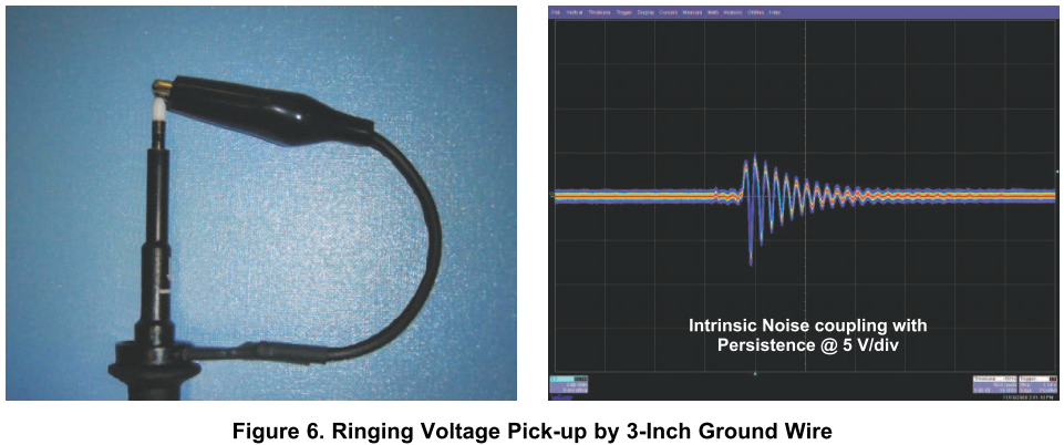
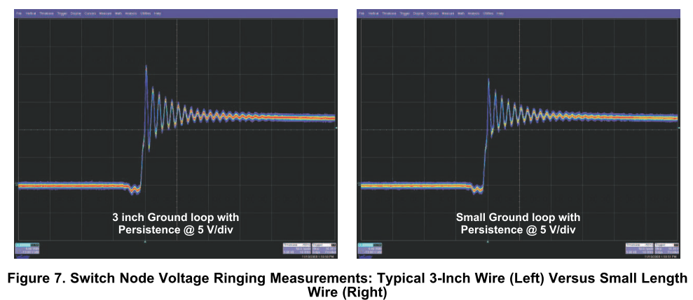
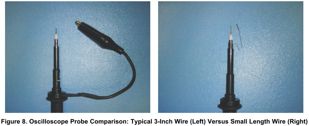
- The ground lead length of an oscilloscope probe is the most important item in properly capturing the peak values of the switch node voltage ringing. Do not use the standard 3-inch long ground wire supplied with the oscilloscope probe. The long wire loop will act as an antenna by picking up any radiated noised emitted by the system board and will yield a higher value of switch node voltage ringing than what is actually seen by the device (see Figure 6 and Figure 7). Instead, use asmall-length ground wire that attaches to the oscilloscope probe tip end (see Figure 8).
- Placement of the oscilloscope tip and ground must be right on the MOSFET leads. Placement anywhere else introduces higher voltage ringing induced by the PCB parasitic inductance.
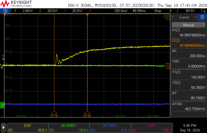
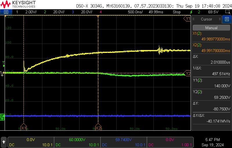
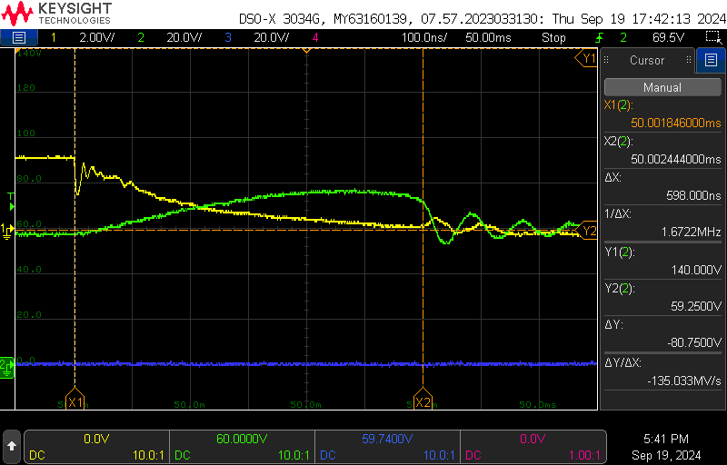
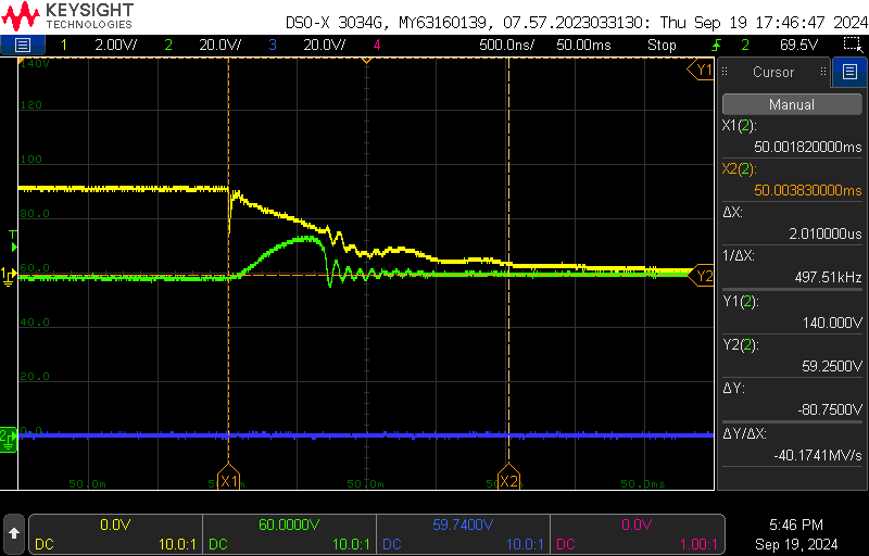
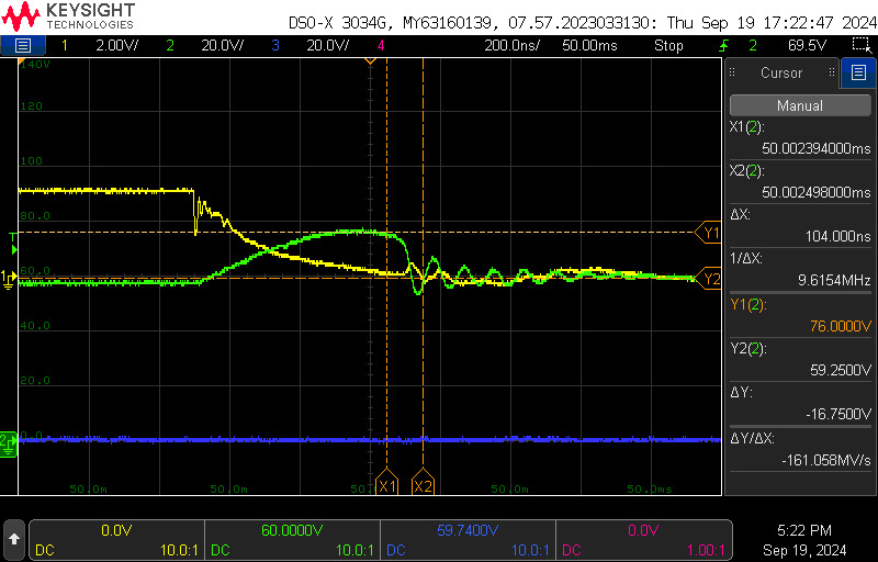
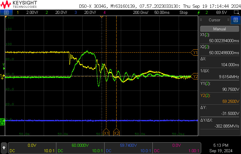
Cgs 对开通关断建立时间的影响
增加了10nF的电容在Vgs电路上:
开通
关断
浅析MOS管导通过程及RC吸收电路设计要点
- https://blog.csdn.net/liangbo1999/article/details/132981000
- https://www.digikey.cn/zh/articles/resistor-capacitor-rc-snubber-design-for-power-switches
转载请注明出处!感谢GISPALAB实验室的老师和同学们的帮助和支持~

 浙公网安备 33010602011771号