
阅记-处理器微架构-Understanding Bandwidth and Latency inside hardware architechture
link:Understanding Bandwidth and Latency - Ars Technica
Understanding Bandwidth and Latency
Ars discusses issues of bandwidth and latency inside hardware architechture.
Introductuion
From the bygone debates over DDR vs. RDRAM to the current controversy over Apple's DDR implementations, one issue is commonly misunderstood in most discussions of memory technology: the nature of the relationship between bandwidth and latency. This article aims to give you a basic grasp of the complex and subtle interaction between bandwidth and latency, so that the next time you see bandwidth numbers quoted for a system you'll be able to better understand how those numbers translate into real-world performance.
This article was written in such a manner that the concepts communicated in it will be applicable to understanding a wide range of systems and parts of systems: from the frontside and memory buses of current P4 and Athlon systems to the buses in Apple's new XServe. Throughout the article, then, I've deliberately avoided getting mired down in the details of specific implementations in hopes that the general concepts will stand out clearly for the reader. The flip side of this simplicity is that for almost every claim I make a technically savvy reader could probably point out various exceptions, workarounds and other caveats peculiar to particular systems and data access scenarios. Nonetheless, I hope that the article will contribute to more informed discussions when bandwidth-based comparisons between different systems come up in forums like Ars's own OpenForum.
The theoretical: peak bandwidth
Most technical people have this sense of bus bandwidth as a single number, attached to a line or a bus, that quantifies how much data the line or bus can carry. In this view bandwidth is seen as an intrinsic, fixed property of the transmitting medium itself, a number that's unaffected by the vagaries of the transmitters at either end of the medium.
When people talk about bus bandwidth this way what they're really describing is only one type of bandwidth: the bus's theoretical peak bandwidth. The peak bandwidth of a bus is the most easily calculated, the largest (read: the most marketing friendly), and the least relevant bandwidth number that you can use to quantify the amount of data that two components (i.e. the CPU and RAM) can exchange over a given period of time. In most product literature this theoretical number, which is rarely (if ever) approached in actual practice, will be cited whenever the literature wants to talk about how much bandwidth is available to the system. Let's take a closer look at how this number is calculated and what it represents.
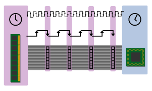
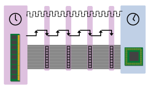
Figure 1
Take a moment to look over the simplified, conceptual diagram above. It shows main memory sending four, 8-byte blocks of data to the CPU, with each 8-byte block being sent on the falling edge (or down beat) of the memory clock. Each of these 8-byte blocks is called a word, so the system shown above is sending four words in succession from memory to the CPU.
(Note that this example assumes a 64-bit (or 8-byte) wide memory bus. If the memory bus were narrowed to 32 bits, then it would only transmit 4 bytes on each clock pulse. Likewise, if it were widened to 128 bits then it would send 16 bytes per clock pulse.)
Think of the falling edges or down beats of the memory bus clock as hooks on which the memory can hang a rack of 8 bytes to be carried to the CPU. Since the bus clock is always beating, it's sort of like a conveyor belt with empty hooks coming by once every clock cycle. These empty hooks represent opportunities for transmitting code and data to the CPU, and every time one goes by with nothing on it it becomes wasted capacity, or unused bandwidth. Ideally, the system would like to see all of these hooks filled so that all of the bus's available bandwidth is used. However, for reasons I'll explain much later, it can be difficult to keep the bus fully utilized.
In addition to the memory clock, I've included the CPU clock at the top for reference. Note that the CPU clock runs much faster than the bus clock, so that each bus clock cycle corresponds to multiple (in this case about 7.5) CPU clock cycles. Also note that there is no northbridge; the CPU is directly connected to main memory for the sake of simplicity, so for now when I use the term "memory bus" I'm actually talking about this combination frontside bus/memory bus.
In the preceding diagram and in the ones that follow, I've tried to represent the amount of time that it takes for memory to respond to a request from the CPU (or latency) as a distance value. The size of the CPU clock cycles will remain fixed in each diagram, while the number of CPU clock cycles (and, in effect, the distance) separating the CPU from main memory will vary. In depictions of systems where memory takes fewer CPU clock cycles to respond to a request for data, memory will be placed closer to the CPU; and vice versa for systems where memory takes more clock cycles to deliver the goods.
Just to show you what I'm talking about, check out the following picture to see how I illustrate a system with a slower bus speed.
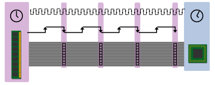

Figure 2
The slower, "longer" bus in the above diagram has a lower peak bandwidth than the faster bus, since it delivers fewer 8-byte blocks in a given period of time. You can see this if you compare the number of CPU clock cycles that sit between the CPU and RAM in the first diagram versus this one. Since the length of the CPU clock cycles has remained fixed in between the two diagrams, you can see that the slower bus takes more time to send data to the CPU because the number of CPU cycles between the CPU and RAM is greater in the second diagram than it is in the first one.
由于 CPU clock cycles 的长度在两个图之间保持固定,因此可以看到较慢的总线将数据发送到 CPU 需要更多时间(第二个图中 CPU 和 RAM 之间的 CPU 周期数比第一个图中的要多)
Now that we've got that straightened out, let's try a bandwidth calculation. If the slow bus runs at 100 million clock cycles per second (100MHz) and it delivers 8 bytes on each clock cycle, then its peak bandwidth is 800 million bytes per second (800 MB/sec). Likewise, if the faster bus runs at 133MHz and delivers 8 bytes per clock cycle, then its bandwidth is 1064 MB/sec (or 1.064 GB/sec).
8 bytes * 100MHz = 800 MB/s
8 bytes * 133MHz = 1064 MB/s
Both of these numbers are theoretical peak bandwidth numbers that characterize the bandwidth of the bus only. Or, to go back to the "hooks" analogy, these numbers simply tell you how many hooks are going by each second. There's quite a bit more to the picture than just the capacity of the bus, though, and once we factor in the capabilities of both the consumer (the CPU) and the producer (the RAM) we'll see that the real-world bandwidth of the system as a whole is usually quite a bit less than the raw capacity of the transmitting medium might at first suggest. The more hooks that go by unfilled (for whatever reason) the greater the real-world bandwidth of the system is diminished.
除了总线的容量之外,还有更多因素,一旦考虑到消费者 (CPU) 和生产者 (RAM) 的能力,就会发现整个系统的实际带宽通常比传输介质(bus)的原始容量要小得多。未填充的 hook 越多(无论出于何种原因),系统的实际带宽减少得越大
One final thing that I should make clear before we move on is that a complete clock cycle consists of one up beat and one down beat. For reasons that will become apparent when we talk about DDR signaling, in my diagrams I've slightly separated the up and down beats, but you can also imagine them fused together.
The practical: sustained bandwidth
In the preceding discussion of peak bandwidth, the bus has been pictured as kind of a one-way fire hose--you turn it on, and data comes pouring out the other end at full blast. The problem with this image, like the problem with peak bandwidth, is that the bus isn't just a dumb conduit for blasting code and data from one end to the other; rather, it's a two-way communications medium. The CPU and RAM talk to each other via the bus, and in this conversation the bus acts like a one-way C.B. radio where only one person can talk at a time. Here's how it works.
Since only one party can use the bus at a time, when the CPU wants to send a request for data it must first request control of the bus. Once it gets control of the bus it can transmit its request, and after its request has been transmitted it relinquishes control. When the RAM receives the request, it goes about finding the proper data and preparing it for transmission back to the CPU. Once the data is ready, the RAM requests control of the bus and then transmits the requested data back to the CPU.
Now, assuming that the CPU's request for control of the bus is granted instantaneously (this isn't always the case), it still takes a certain amount of time for the CPU's request for data to reach RAM. Furthermore, it also takes a certain amount of time for RAM to fill that request, and a certain amount of time for the requested data to arrive back at the CPU. All of these delays taken together constitute the system's read latency. In short, the read latency is the time gap between when the processor places a request for data on the frontside bus (FSB) and when the requested data arrives back on the FSB.
读取延迟=cpu请求控制总线到被接受的时间+CPU数据请求到达RAM的时间+RAM接受请求并填充数据的时间+RAM请求控制总线到被接受的时间+数据放到总线的时间(数据到达CPU花费的时间)
简而言之,读取延迟是处理器在前端总线 (FSB) 上发出数据请求与请求的数据返回 FSB 之间的时间间隔。
Depending on how many different buses separate the CPU from RAM and how long it takes the RAM to respond to a request for data, this read latency can grow relatively large. If we just pick a number and say that the read latency for the simple system pictured in our diagrams is 3 bus cycles, then this means that each time the CPU transmits a request for data it has to wait three cycles for that data to arrive. If the CPU made 100 requests for data, then that would mean 300 wasted cycles, or empty hooks. That's a lot of wasted capacity. In fact, it should be obvious that if the system is structured such that only one out of every four of the bus's cycles can actually be used (i.e. 1 full cycle + 3 empty cycles = 1 out of every 4 cycles is usable), then at best the system will be able to operate at only 1/4 of its peak bandwidth. That's right: with a 3-cycle read latency the best bandwidth utilization that the simple system in our example can possibly achieve is a measly one quarter of its theoretical peak.
The maximum possible bandwidth that a system can achieve after read latency is taken into account is called sustained bandwidth.
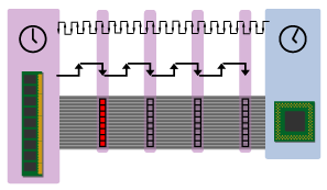
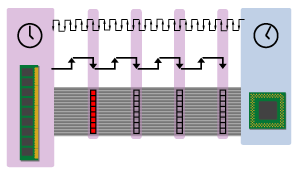
Figure 3
In figure 3, that one red clock beat is the only beat with a group of 8 bytes on it; the other three beats are empty due to read latency. So the bus pictured above is only 1/4 full. Since we previously calculated the theoretical bandwidth of an 8-byte, 100MHz bus as 800 MB/s, it's sustained bandwidth is 1/4 of that number, or 200 MB/s.
如Figure3,总线宽度是64位(8字节),读取8字节消耗了4个总线周期,其中read latency为3clock,数据放到总线的消耗1clock(数据抵达cpu),那么实际峰值是最大峰值的1/4
Latency and bursting
In order to get around the bandwidth-killing effects of read latency, real systems have a host of tricks for keeping the bus full in spite of the delays outlined above. One of the oldest and most important of these tricks involves minimizing the number of read requests the CPU must issue in order to bring in a certain amount of data. If RAM can anticipate the data that the CPU will need next and send it along with the data that the processor has just requested, then the CPU won't have to issue read requests to get that data since it'll already have it on hand. In this section, I'll describe this technique in a bit more detail so that you can understand its impact on bandwidth.
To recap a bit from both my article on caching and the Ars RAM Guide, when the CPU requests a specific byte from memory the memory system returns not only the requested byte but also a group of its contiguous neighbors, all under the expectation that those neighboring bytes will be needed next. See, the requested byte has to be written into the CPU's L1 cache, and the L1 cache will only accept an entire cache line from the memory system and not an individual byte. So the memory system sends out a cache line consisting of the requested byte and its contiguous neighbors in memory, and that cache line travels across the bus and is written to the L1 cache.
In all of the examples and diagrams given so far, the line size of the CPU's cache line is assumed to be 32 bytes, or four, 8-byte words. So when the L1 cache in the preceding diagrams requests data (note that the cache isn't explicitly depicted--it's presumed to be part of the CPU), it's actually asking for 32 bytes at once. Since the memory bus is only 8 bytes wide then the memory system must break that request up into a series of four, 8-byte chunks and send those chunks in sequence over the bus.

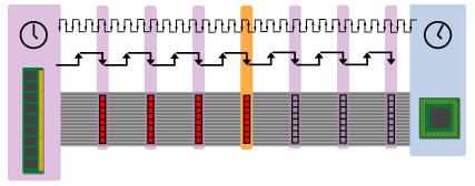
Figure 4: Bursting a cache line
The orange clock pulse above designates what's called the critical word (remember, 1 word = 8 bytes). The critical word is so called because it contains the specific byte that the CPU requested. With most SDRAM architectures (but not RAMBUS), the memory system places the critical word on the bus first so that it's the first to arrive at the CPU. The rest of the cache line then comes trailing behind it at a rate of one line per clock beat.
If you'll recall from the RAM Guide, an SDRAM operating in burst mode can fire a series of words onto the bus, one on each consecutive beat of the clock, in response to a request for data. So the memory depicted above is bursting onto the bus the four blocks that make up the requested cacheline. In the diagram above, there's a gap of 3 clock cycles between when the request was sent and when the first of the four words appears on the bus--that's our system's 3-cycle read latency. So the first (or "critical") word has a latency of 3 cycles, and each subsequent word has a latency of one cycle. (When you see DRAM latency timings described as 3-1-1-1, this is what they're talking about.) The total time that it takes to burst the entire cache line (all four 8-byte blocks) onto the bus is 3 + 1 + 1 + 1 = 6 cycles.
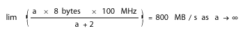
In order to calculate the maximum sustained bandwidth of a system with a four-cycle burst, we must base our calculation on the total number of cycles it takes to transmit all four words of the 4-word cache line. In the system described above, four words (or 4 x 8 = 32 bytes) are transmitted every 6 clock cycles. So on a 100 MHz bus the maximum sustained bandwidth would be 533 MB/s. Here's the calculation written out:
4 words x 8 bytes x 100MHz/(3 clocks + 1 clock + 1 clock + 1 clock) = 533 MB/s
优化技巧:预取,也就是Cache
假设总线宽度是64位(8字节),cacheline是32字节,read latency为3周期,那么实际需要的周期数为:3+1+1+1+1(文中少算了一个?),即带宽利用率由1/4变为4/7
This number is significantly lower than the 800 MB/s peak bandwidth that we calculated earlier. As you can see, when those empty clock cycles that are lost due to latency are factored into the bandwidth calculations, the entire system turns out to have much lower throughput than it would were latency not a factor.
It's important to understand that the system's sustained bandwidth is not being bounded by the bandwidth of either the producer or the consumer. The DRAM could very well be capable of putting out 8 bytes on every single clock pulse for an indefinitely long time, and the CPU could likewise be capable of consuming data at this rate indefinitely. The problem is that there's a turnaround time in between when the request is sent out and when the data is produced. This turnaround time isn't so much the fault of the bus for not getting the CPU's request in fast enough as it is the fault of the DRAM for not being able to fill it instantaneously. But before I explain why the DRAM is so slow in responding to requests for data, I need to clear something up.
A Clarification
My analogies and diagrams, with the empty "hooks" or clock beats visually marking out the system's latencies, perhaps encourages the erroneous idea that the bus is somehow multiple bus cycles in length and that the bus clock propagates down the bus in such a manner that there are multiple clock pulses and multiple words on the same bus at the same time. While this is actually true of RDRAM systems, it is not true of SDR and DDR DRAM systems. In the kinds of systems we're looking at in this article (SDR and DDR), the bus is physically only one bus clock in length. This means that the bus transmits only one word at a time, and not four or however many I've depicted as being on the bus.
Since the bus really only "contains" one cycle at a time, instead of thinking of those empty bus cycles in my diagrams as empty cycles propagating along the bus towards the CPU, it might be better to think of them as moments when that 1-cycle-length bus's clock was ticking but nothing was being placed on it.
The real killer: DRAM access latencies
The largest factor affecting read latency is by far the DRAM's response time, or access latency. The average access latency of a DRAM hasn't decreased very much in the past decade relative to the average CPU speed, so this problem is not going away. In fact, in an important sense it's getting worse. Let me explain why.
The row access time (tRAC) for DRAM is the amount of time between when the DRAM's RAS line falls and when valid data is available on its output pins, and this number is a big factor in DRAM access latency. (For more on this, see the Ars RAM Guide). As bus clock cycle times and CPU clock cycle times get ever shorter compared to the DRAM's row access time, then the more bus clock and CPU cycles will be wasted waiting for the DRAM to respond with data.
Consider DRAM with row access time of 60ns. If this DRAM is coupled with a 1GHz CPU (@ 1 GHz the clock cycle time = 1 ns), then 60 clock cycles of CPU time will have gone by from the time the row address is asserted to when the data is placed on the memory bus. This is quite a long time, especially considering the fact that we haven't even added in the additional delays which result from first transmitting the addresses to RAM and then transmitting the data back to the CPU.
A 60ns DRAM with a 1GHz CPU is really an exaggerated example, though. Fast DRAM latencies are more on the order of 30-40ns. Still, 30ns is 30 cycles of a 1GHz CPU's time, and it's 60 cycles of a 2 GHz CPU's time. Furthermore, as memory bus speeds increase then stagnating row access times will mean more bus cycles worth of delay for each memory access. This means that more bus cycles will go by empty and more bandwidth will be wasted.
Making better use of bus bandwidth: data streaming
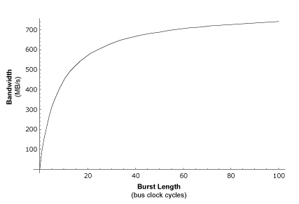
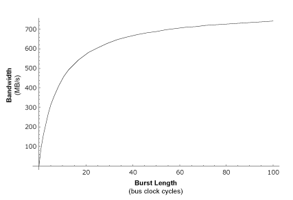
If you're perceptive and you gave my previous sustained bandwidth calculations more than a cursory glance, then you probably noticed that increasing the length of the bursts from four beats to an indefinitely large number of beats would allow you to approach the theoretical peak bandwidth. In other words, because the initial read latency remains fixed, then as you fill more and more consecutive clock beats after the initial word the ratio of used cycles to unused cycles starts to improve. So if after an initial latency of 3 cycles you're able to fill the next 100 consecutive clock beats with data, without a single gap or break, then the ratio of empty cycles (three) to full cycles (one hundred) over the course of that block of 103 cycles begins to pretty good.
The following calculations should show you the math in action:
4 words * 8 bytes * 100MHz/(3 clocks + 1 clock + 1 clock + 1 clock) = 533 MB/s
5 words * 8 bytes * 100MHz/(3 + 4) = 571 MB/s
6 words * 8 bytes * 100MHz/(3 + 5) = 600 MB/s
7 words * 8 bytes * 100MHz/(3 + 6) = 622 MB/s
For those of you who remember some basic calculus, the limit function for this would look as follows:

Here's a graph that illustrates the way this function works:
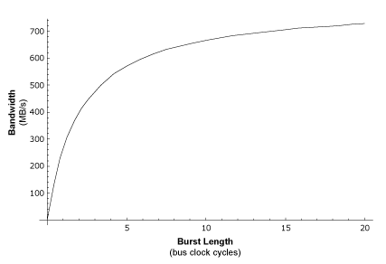

Graph 1: Bandwidth vs. Burst Length
The above graph should make it clear that as burst length increases so does sustained bandwidth. For extremely large burst lengths the sustained bandwidth approaches (but never achieves) the peak theoretical bandwidth.
Data streaming on modern processors
It would be nice if burst length's could grow indefinitely large, in real-world systems there are factors that limit their size. In this subsection we'll look at some of those factors and how modern bus protocols work around them.
When a bus master requests the bus, it can only "lease" the bus for a fixed amount of time before it has to release it so that another bus master can use it if needed. Forcing bus masters to renew their lease on the bus after a fixed amount of time ensures that all of the other masters attached to the bus get a chance to use it. A lease that's granted to the CPU for the transfer of data is called a data tenure. Data tenures come in fixed, predefined time slices, and for Motorola's buses a data tenure is either a 1-beat transfer of a single byte, a 1-beat transfer of an entire word, or a 4-beat transfer of an entire 4-word cache block. At the end of each data tenure on the older 60x bus (the bus for the G3), the bus master had to relinquish control of the bus for at least on cycle. This meant that the 60x bus was inefficient for streaming large chunks of data, like a series of cache blocks, because there had to be at least one wasted bus cycle (which translates into multiple wasted CPU cycles) in between each cache block transfer.
Both the MPC7455's and the P4's bus protocols support data streaming. This feature allows the G4's newer MPX bus to continually stream data over the bus at the rate of 8 bytes per beat until some other bus master interrupts the stream by requesting the bus. This makes much more efficient use of bus bandwidth, and allows the G4 to approach the bus's theoretical peak bandwidth.
Latencies in real-world systems
Now let's take a look at a graph that scales out to much longer burst lengths than the 20-beat maximum in the previous graph.
Graph 2: Bandwidth vs. Burst Length
One thing you should know about this graph is that even though its curve may appear to be steeper than that of the previous graph, this is only because the previous graph shows fewer burst lengths (only up to 20). The graph shown above is actually much slower to ramp up to the peak bandwidth than the previous graph, and this is because I've used a 9-cycle memory read latency instead of the 3-cycle latency in the former graph. The 9-cycle latency number more accurately reflects the kind of latency seen by a real-world system. Let's look at why this is.
In systems where memory is connected directly to the CPU (whether main memory or a backside L2 or L3 cache), data takes only one bus clock cycle to travel between the memory and CPU. As I've said before, in the simplified diagrams above the data only appears to take multiple clock cycles to traverse the bus. This was just my way of depicting the fact that the CPU has to wait multiple bus cycles for a request to be filled, so as far as the CPU is concerned the bus appears to be multiple cycles in length. In reality, we could break down the hypothetical 3-cycle latency of our simplified system as follows:
| Cycle # | Event |
| 1 | The CPU's request for data travels across the bus to the DRAM. |
| 2 | The DRAM fills the CPU's request. |
| 3 | The requested data travels back across the bus to the CPU. |
Of course, as should be clear from the preceding section on DRAM latencies, at bus speeds of 100MHz or better real DRAM takes more than one cycle to fill a request. So a more realistic description of read latency in a real system might look as follows:
| Cycle # | Event |
| 1 | The CPU's request for data travels across the bus to the DRAM. |
| 2-5 | The DRAM fills the CPU's request. |
| 6 | The requested data travels back across the bus to the CPU. |
As I've pointed out earlier, the preceding diagrams showing the memory and CPU directly connected by a single bus have been simplified in order to make the basic concepts clear. In the kinds of PC systems that we usually cover at Ars, the CPU and main memory are not directly connected. (This may change in the future, though.) Instead, the north bridge of the core logic chipset sits in between the CPU and RAM, playing traffic cop by routing information in between the CPU, RAM, and the other parts of the system.
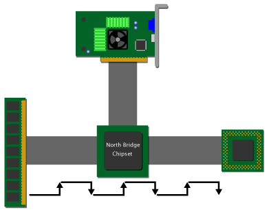
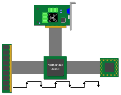
Figure 5
A set-up like the one depicted above adds two cycles of latency to a DRAM read: one cycle for the request to travel across the frontside bus to the northbridge, and one cycle for the northbridge to route the request from the FSB interface to the memory bus interface. As is illustrated in the diagram, this means that the request spends a total of 3 cycles just traveling to the DRAM, and then the data has to spend another 3 cycles traveling back to the CPU. The following chart breaks down the latencies for a system like the one pictured above:
| Cycle # | Event |
| 1 | The CPU's request for data travels across the FSB to the DRAM. |
| 2 | The chipset transfers the request from the FSB to the memory bus. |
| 5-8 | The DRAM fills the CPU's request. |
| 9 | The chipset transfers the request from the memory bus to the FSB |
| 10 | The requested data travels back across the FSB to the CPU. |
So in more complex systems the DRAM read latency increases simply because of the way the system is laid out. Furthermore, when other devices are contending via the northbridge for access to the DRAM, it's possible that the CPU will have to wait even longer to have a given request serviced if the DRAM is busy doing other things, thus adding more dead bus cycles to the read latency. The following chart illustrates the kind of detrimental effects that increases in read latency have on sustained system bandwidth.
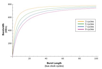

Graph 3: bandwidth vs. burst length at different latencies
The different color curves in the above graph show how the bandwidth of systems with different read latencies ramps up in relation to burst length. The higher the read latency, the longer the burst length has to be before a given amount of sustained bus bandwidth can be attained. So systems with higher read latencies ramp up more slowly than those with lower read latencies. It should be obvious, then, that DRAM read latencies are a huge obstacle to achieving efficient bandwidth usage.
There are other obstacles as well. As I noted previously, the average burst length is not unlimited in a real-word system. In real systems there are multiple components vying for the use of the system memory, including I/O components, multiple CPUs, etc. For instance, if there are two CPUs trying to stream a large amount of data from memory (e.g. both CPUs are running data-intensive Altivec code) then the DRAM must alternate between servicing two sets of requests, which means alternating data tenures. And if each processor is reading data from a different row, then there will be dead cycles in between each processor's data tenure as the DRAM switches rows. Again, these dead bus cycles mean that bandwidth is being wasted. Even worse is the fact that one dead bus cycle can translate into multiple dead CPU cycles if the CPU can't find anything to busy itself with while waiting on the requested data.
Increasing Bandwidth
In the preceding sections, I touched on only a few of the available techniques that some systems use for making more efficient use of available bandwidth. There are so many more that could be covered, like data prefetching, for instance. However, I've discussed many of these techniques here and there in previous articles, so I'll leave off talking about them for now and take up another topic. In this section, we'll switch gears and explore some techniques for adding more bandwidth to the bus itself.
A faster bus
The ideal way to get more bus bandwidth is to increase the speed of the bus. Increasing the bus speed adds more down beats (or "hooks", in our analogy) per second to the bus. More down beats per second means more opportunities per second for sending out code and data. Thus doubling a bus's clock speed also doubles its theoretical peak bandwidth.
More beats/sec also means that each bus cycle translates into fewer CPU cycles, which means that from the CPU's perspective RAM looks "closer" since it has to wait less time to get its requests filled. And of course decreasing the amount of time the CPU has to wait for data is the primary goal of memory subsystem designers.
A wider bus
Another common way to increase bus bandwidth is to increase the width of the bus. If you double a bus's width while keeping its clock speed the same, then although down beats come by at the same rate as before you can place twice as much data on each beat. So for the 8-byte bus + 32-byte cache line system I've been using as an example, if we doubled the bus width to 16 bytes then it would take only two bus cycles to transfer an entire cache line (as opposed to four cycles in the initial example).
Though doubling with width of the bus also doubles the theoretical peak bandwidth, it's a less desirable way to do so than doubling the clock rate. This is because when you double the clock rate the system's initial read latency (calculated in terms of CPU cycles) decreases, while when you double the bus width this latency stays the same. So in a system with a faster bus, it takes less CPU time for RAM to return the critical word than it does on a system with a slower but wider bus.

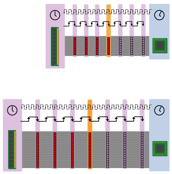
Figure 6: fast bus vs. slow bus
The diagram above illustrates how a faster but narrower bus returns the critical word more quickly to the CPU than a slower but wider one. Since the critical word is the one that the CPU is waiting on at that very moment, it's always best to get the critical word in as fast as possible.
Of course, it should be noted that the above diagram presumes that the RAM attached to the faster bus can actually cough up the critical word in a shorter amount of time than the RAM attached to the slower but wider bus. This only works if the faster system's RAM has a sufficiently short access latency. In some cases, when designers increase the speed of the bus without also using RAM with a lower access latency, it winds up taking more of the shorter cycles to get the critical word in. This is similar to the situation, discussed below, with DDR buses.
For some applications, especially media apps that do lots of data streaming over the bus, the critical word isn't quite so critical in terms of real-world performance. Such systems benefit more from high sustained bandwidth than they do from getting the critical word out quickly, which is why RDRAM works so well with such apps in spite of the fact that it does not do critical word first bursting. In systems designed to run applications where the critical word's latency isn't quite so important, it's cheaper and easier for a system manufacturer to double the bus width than it is to increase the bus frequency. This is why very wide memory buses have become so popular as processor frequencies increase. It's tough to scale memory bus frequency to match ever higher CPU speeds, so system makers compensate by widening the bus.
Doubling the data rate
A relatively easy way to jack up a bus's peak bandwidth is by sending data on both the rising and falling edges of the clock. It's much easier to implement such a double data rate (DDR) bus than it is to actually double the clock rate of a bus. So DDR allows you to instantly double a bus's peak bandwidth without all the hassle and expense of a higher frequency bus.
Let's take a look at a DDR bus.
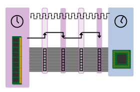

Figure 7: DDR bus
Since this bus can carry data on the clock's rising and falling edges, it's able to transfer all four beats of our 32-byte cache line in only two clock cycles, or half the number of clock cycles as the SDR bus in our previous example.
Of course, just because DDR allows you to easily double a bus's peak bandwidth, this doesn't mean that the bus's sustained bandwidth is doubled as well. In the following graph, the blue curve represents a 200MHz SDR bus, while the red curve represents a 100MHz DDR bus.

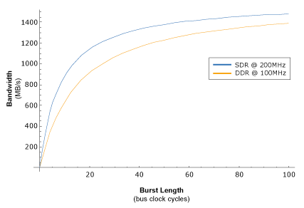
Graph 4: Bandwidth vs. burst length
Notice how the blue curve ramps up much faster than the red curve. This is because the 200MHz SDR bus's read latency is much shorter than that of the 100MHz DDR bus. In other words, doubling the data rate does not affect read latency, which means that it also does not affect the amount of time it takes for the CPU to get the critical word. Take a look at how this works:

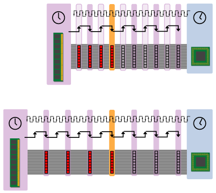
Figure 8
The top figure shows a DDR system, while the bottom figure shows an SDR one. The DDR system gets all four beats of the cache line to the CPU faster, but the critical word arrives at the exact same time as an SDR system with the same bus clock rate. In the end, while DDR signaling affords real increases in peak and sustained bandwidth, it isn't without its shortcomings. The ideal will always be a combination of increased bus frequencies and decreased DRAM access latencies.
Conclusions
There are many other factors playing into sustained bandwidth that I haven't covered above. For instance, I haven't really discussed other types of non-data bus traffic (e.g. address traffic, cache snoop traffic, command traffic etc.) that can take up a significant portion of a system's bandwidth and thereby limit the amount of bandwidth available for use by the CPU for receiving data. In this respect, packet-based bus protocols, like RDRAM's memory bus protocol or the PowerPC 970's frontside bus protocol, are probably the worst offenders. Although such protocols usually run on a much faster bus, command and address traffic can take up a relatively greater fraction of available bus bandwidth than such traffic would on a simpler bus. Nonetheless, the preceding discussion should provide a useful framework for understanding how the specifics of various implementations impact sustained bandwidth and performance.
Revision History
| Date | Version | Changes |
| 11/6/2002 | 1.0 | Release |
| 12/4/2002 | 1.1 | Some minor clarifications; I changed the maximum burst lengths on the graphs from a ridiculously long 400 beats to a slightly less ridiculously long 100 beats. (Please note that these are idealized numbers intended to prove a point.) |
- Understanding Bandwidth and Latency
- Introductuion
- The theoretical: peak bandwidth
- The practical: sustained bandwidth
- Latency and bursting
- A Clarification
- The real killer: DRAM access latencies
- Making better use of bus bandwidth: data streaming
- Latencies in real-world systems
- Increasing Bandwidth
- Conclusions
- Revision History
- 小结
小结
In addition to the memory clock, I've included the CPU clock at the top for reference. Note that the CPU clock runs much faster than the bus clock, so that each bus clock cycle corresponds to multiple (in this case about 7.5) CPU clock cycles. 处理器比外围设备处理速度快得多
read latency
读取延迟=cpu请求控制总线到被接受的时间+CPU数据请求到达RAM的时间+RAM接受请求并填充数据的时间+RAM请求控制总线到被接受的时间+数据放到总线的时间(数据到达CPU花费的时间)
简而言之,读取延迟是处理器在前端总线 (FSB) 上发出数据请求与请求的数据返回 FSB 之间的时间间隔。
如Figure3,总线宽度是64位(8字节),读取8字节消耗了4个总线周期,其中read latency为3clock,数据放到总线的消耗1clock(数据抵达cpu),那么实际峰值是最大峰值的1/4
如何优化? 预取,也就是Cache
假设总线宽度是64位(8字节),cacheline是32字节,read latency为3周期,那么实际需要的周期数为:3+1+1+1+1,即带宽利用率由1/4变为4/7
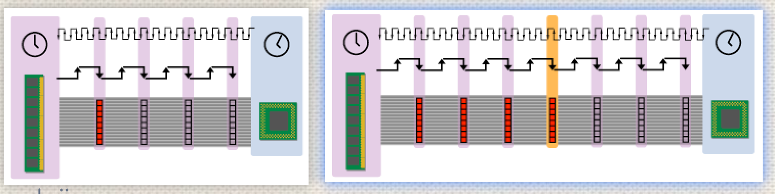
(图中红色标识的数据表示数据被放到总线上)
RAM access data latency
回顾【读取延迟】的计算公式,其中【RAM接受请求并填充数据的时间】是最大因素,且由于cpu的处理速度和总线的处理速度的提高程度高于RAM准备数据的处理速度的提高程度,导致更多的cpu和bus周期数被浪费
如何优化?data streaming
通过计算公式3+1+1+1+1.... 显然如果read latency后面是连续的数据被放到总线,那么read latency就可以被弱化,现代处理器通过一种"data streaming"的机制来达到对应目的
Latencies in real-world systems
真实系统中,read latency不仅仅只有3周期,详见文中描述
Increasing Bandwidth
A faster bus、A wider bus、Doubling the data rate(在 clock的 rising edge 和 falling edges 上发送数据)
总而言之,选择更大cache、更快ram-access-data、更快bus频率、更高bus位宽、支持clock上下沿传输数据
本文来自博客园,作者:LiYanbin,转载请注明原文链接:https://www.cnblogs.com/stellar-liyanbin/p/18646922


【推荐】国内首个AI IDE,深度理解中文开发场景,立即下载体验Trae
【推荐】编程新体验,更懂你的AI,立即体验豆包MarsCode编程助手
【推荐】抖音旗下AI助手豆包,你的智能百科全书,全免费不限次数
【推荐】轻量又高性能的 SSH 工具 IShell:AI 加持,快人一步
· TypeScript + Deepseek 打造卜卦网站:技术与玄学的结合
· Manus的开源复刻OpenManus初探
· 三行代码完成国际化适配,妙~啊~
· .NET Core 中如何实现缓存的预热?
· 如何调用 DeepSeek 的自然语言处理 API 接口并集成到在线客服系统