Architecture of Modern CPU
In this blog, we will take a look on the architecture of modern CPU, from a programmer's perspective.
Intro
Let's review how an instruction is executed on the CPU.
Each computer's CPU can have different cycles based on different instruction sets, but will be similar to the following cycle:
- Fetch Stage: The next instruction is fetched from the memory address that is currently stored in the program counter and stored into the instruction register. At the end of the fetch operation, the PC points (i.e. register
EIP) to the next instruction that will be read at the next cycle.- Decode Stage: During this stage, the encoded instruction presented in the instruction register is interpreted by the decoder.
- Read the effective address: In the case of a memory instruction (direct or indirect), the execution phase will be during the next clock pulse.
- Execute Stage: The control unit of the CPU passes the decoded information as a sequence of control signals to the relevant functional units of the CPU to perform the actions required by the instruction, such as reading values from registers, passing them to the ALU to perform mathematical or logic functions on them, and writing the result back to a register.
Therefore, there are at least 3 components in abstraction of CPU core, fetch-decode unit (control unit), ALU (execution unit), a set of registers.
Cache
In modern CPU, cache is one of the vital components.
As the figure shown, it's a simple abstraction of a modern CPU, from the perspective of 3-level cahce.
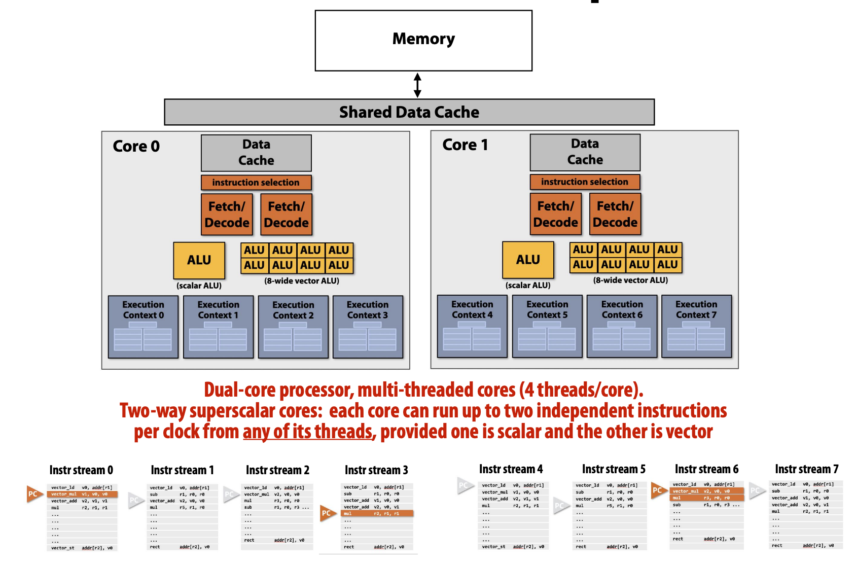
- A CPU can have multiple cores.
- In each core, L1-cache and L2-cache is exclusive, they won't be shared with other cores. But L3-cache is inclusive, it's shared by all cores.
- There are two types of L1-cache, instructions L1-cache and data L1-cache, i.e.
IL1andDL1, shown as follows.
- There are two types of L1-cache, instructions L1-cache and data L1-cache, i.e.
- In each core, there is at least one set of registers, to store the state of thread/process.

NUMA
NUMA is "Non-Unified Memory Access".
In our common sense, all the DRAM memory have equal status in front of each CPU core. But in fact, that's not true.
For most modern multi-processors, they are NUMA architecture. Hence the memory access latency depends on the memory location relative to the processor.
Suppose there are multiple physical CPUs on one machine. (Hint: For most of PCs, laptops, there is only one physical CPU. But for some servers or mainframes, there may be multiple CPUs on one machine.)
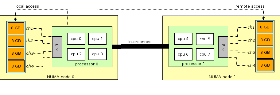
All the main memory (DRAM memory) can be "seen" by all CPUs (and all cores). But for each physical processor, there are two types main memory - "local" and "remote". Accessing the "local" memory is faster than the "remote" memory.
For more details, please refer to Non-uniform memory access. In fact, NUMA will not be covered very much in this blog.
Q&A
- How many CPUs on my machine? -
cat /proc/cpuinfo | grep "physical id" - How many cores in my CPU?
cat /proc/cpuinfo | grep "cpu cores", orcat /proc/cpuinfo | grep "core id"
- What is the max-number of parallel threads at the same time? -
grep "processor" /proc/cpuinfo - Command
lscpuwill list information of CPU.
That is to say, CPU > Core > Processor.
CPU Architecture
In this section, the evolution of CPU architecture is introduced.
- Single core - the most ancestral one, a scalar core
- Parallelized core - superscalar and SIMD
- Multi-cores
- GPU and SIMT
Single Processor
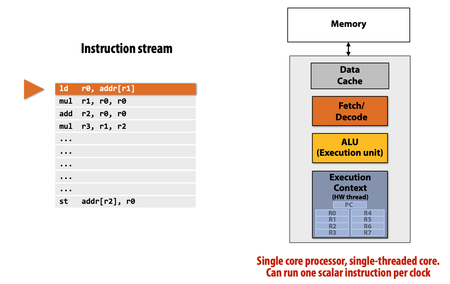
In the most simple processor, it's single, execute the instructions stream one by one.
- Fetch/Decode Unit: Determine what instruction to run next.
- Execution Unit (ALU): Performs the operation described by an instruction, which may modify values in the processor’s registers or the computer’s memory.
- Context (Registers): maintain program state: store value of variables used as inputs and outputs to operations
Superscalar Core

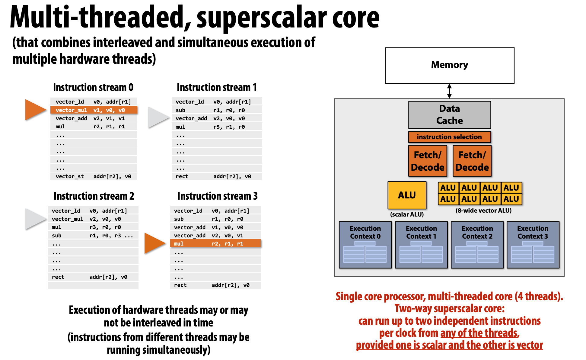
- We can put two (or more) fetch-decode units and ALUs in one core.
- If there are two instructions (e.g.
mulandaddabove), they are independent, then they can be executed at the same time.
However, the Superscalar Core still has ONE instruction stream and ONE data stream (we want more).
Why we call such core "super-scalar" ?
Refer to: https://en.wikipedia.org/wiki/Superscalar_processor
- A scalar processor, which can execute at most one single instruction per clock cycle.
- a super-scalar processor can execute more than one instruction during a clock cycle by simultaneously dispatching multiple instructions to different execution units on the processor.
For example,
for (i = 1 to 10)
{
    a[i] += i;
    b[i] *= i;
}
With single processor, the code above will cost 20 clock cycles. But with superscalar core, it will cost 10 clock cycles.
SIMD
SIMD means "Single Instruction Multiple Data stream".
With SIMD technique, we can perform one instruction on multiple data streams (i.e. different ALUs).
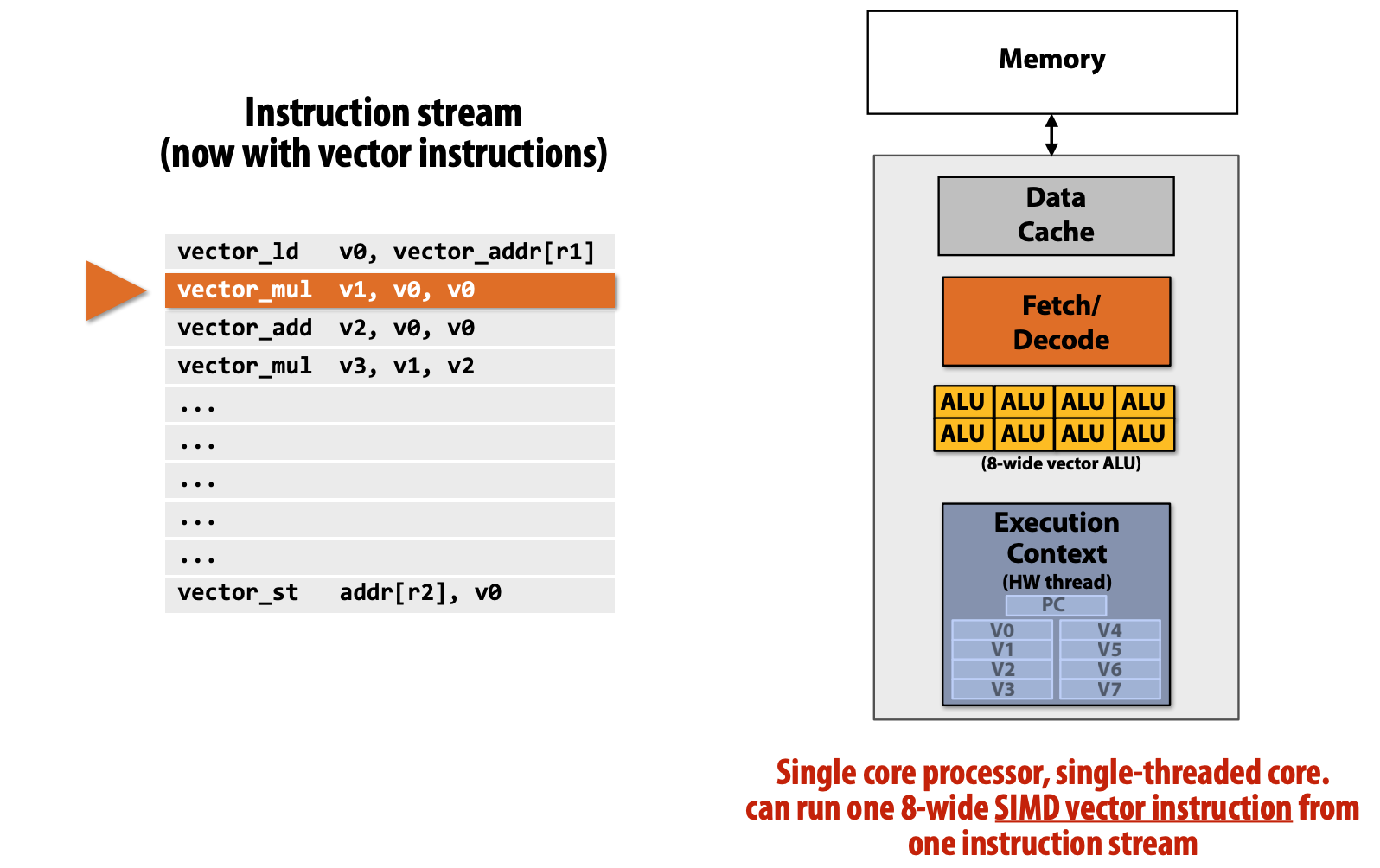
What's the difference with "Superscalar Core"?
- In above example, superscalar core has two fetch-decode units and two ALUs, they execute different instructions at the same time.
- However, SIMD here has ONE fetch-decode unit. It executes same instructions on different data streams (ALUs).
For example,
for (i = 1 to 10)
{
    a += i;
    b += i;
}
With single processor, the code above will cost 20 clock cycles. But with SIMD, it will cost 10 clock cycles.
Scalar + SIMD
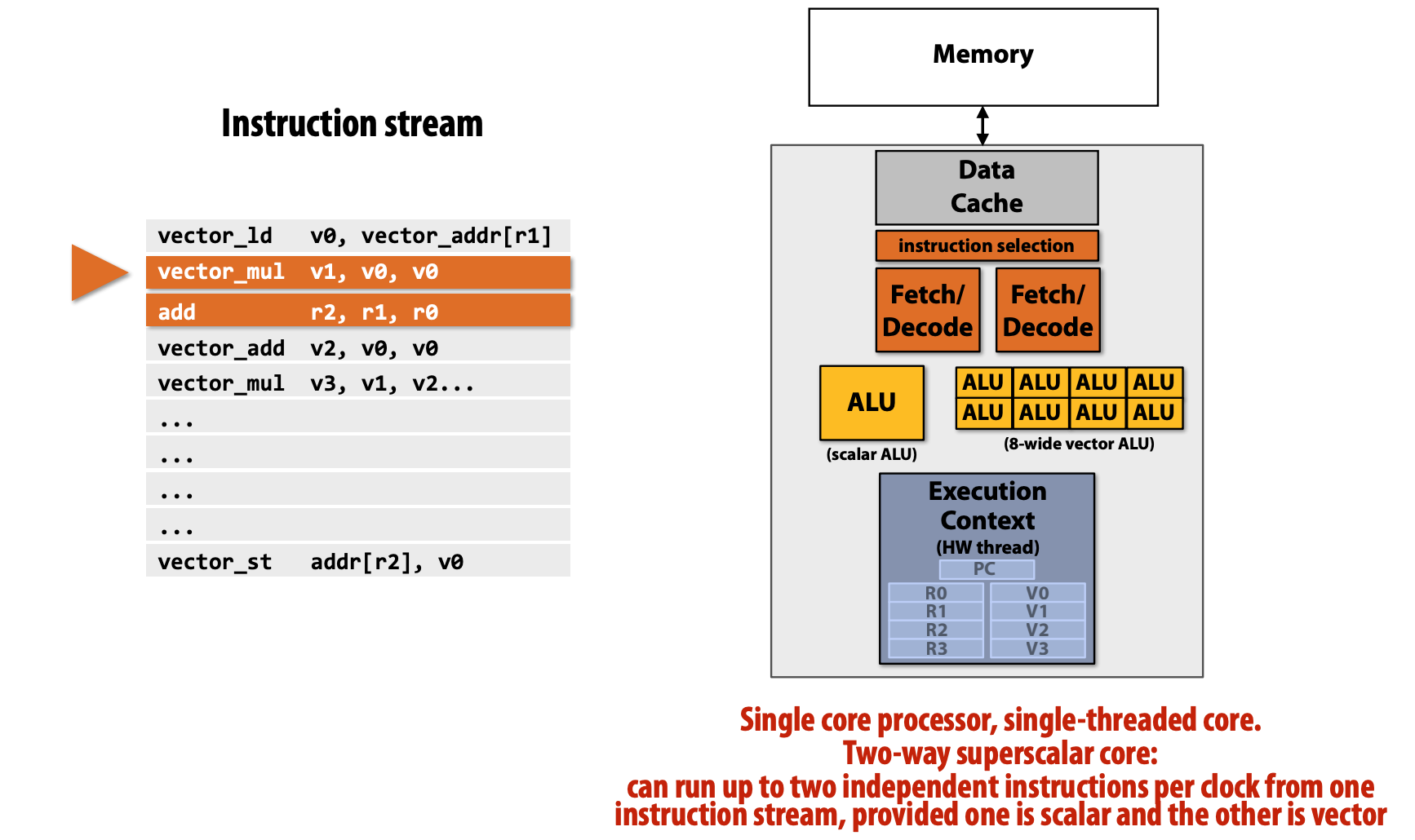
Scalar ALU is similar to "single processor". Here we put one "single core" and "SIMD core" together.
Multi-threaded Core
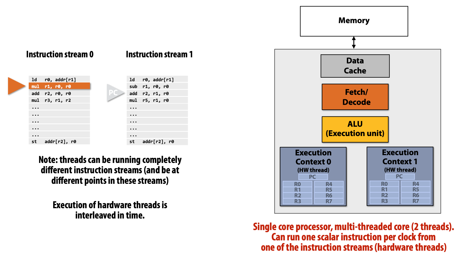
Multi-threaded + Superscalar
Multi-cores, with multi-threaded, superscalar cores
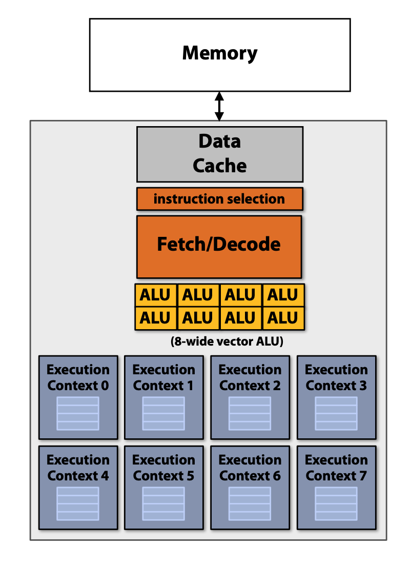
GPU and SIMT
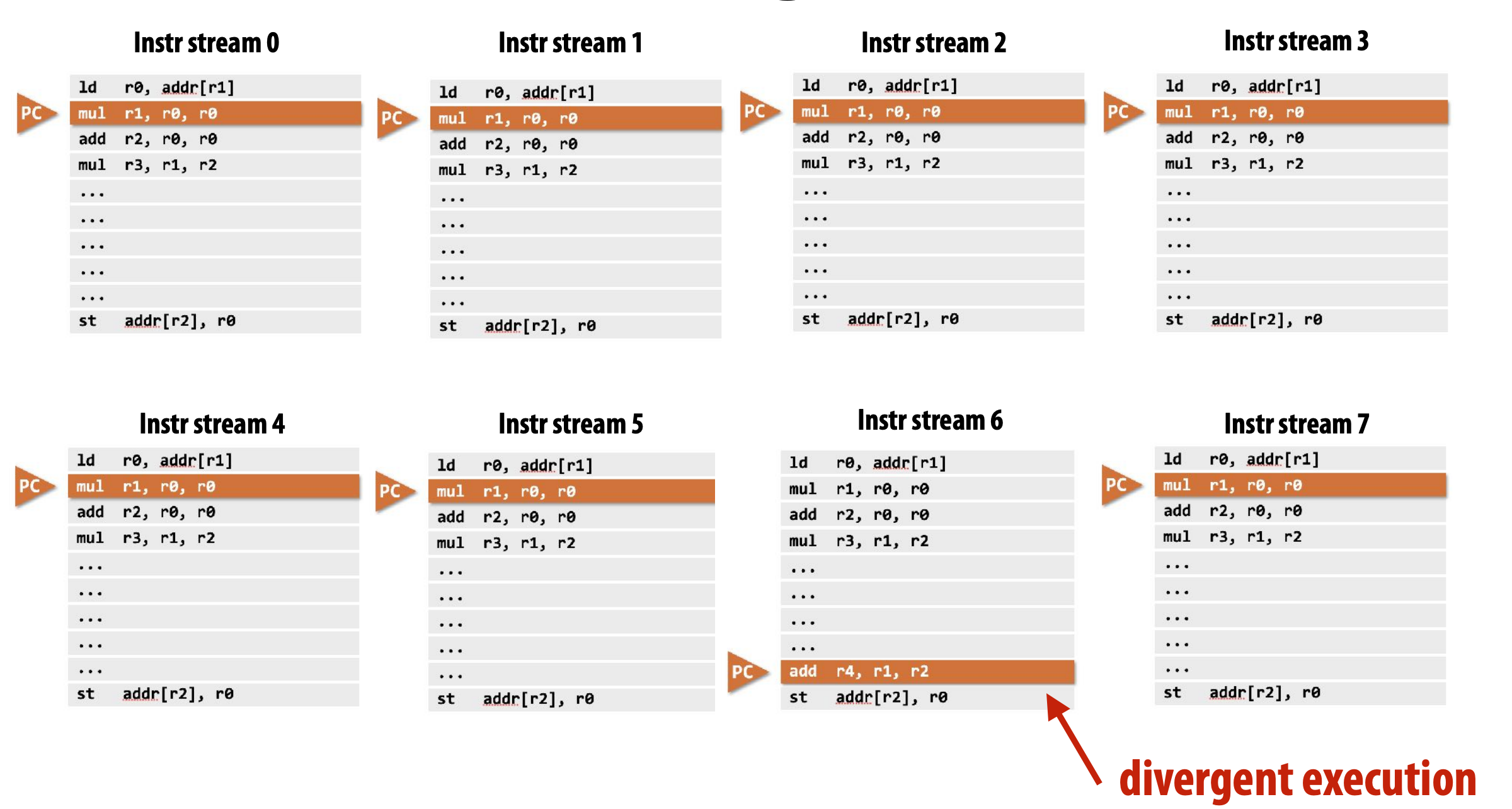
SIMT means "Single Instruction Multiple Threads".
- Many modern GPUs execute hardware threads that run instruction streams with only scalar instructions.
- GPU cores detect when diferent hardware threads are executing the same instruction, and implement simultaneous execution of up to SIMD-width threads using SIMD ALUs.
- Here ALU 6 would be "masked off" since thread 6 is not executing the same instruction as the other hardware threads.
| GPU Abstraction | GPU Threads |
|---|---|
 |
 |
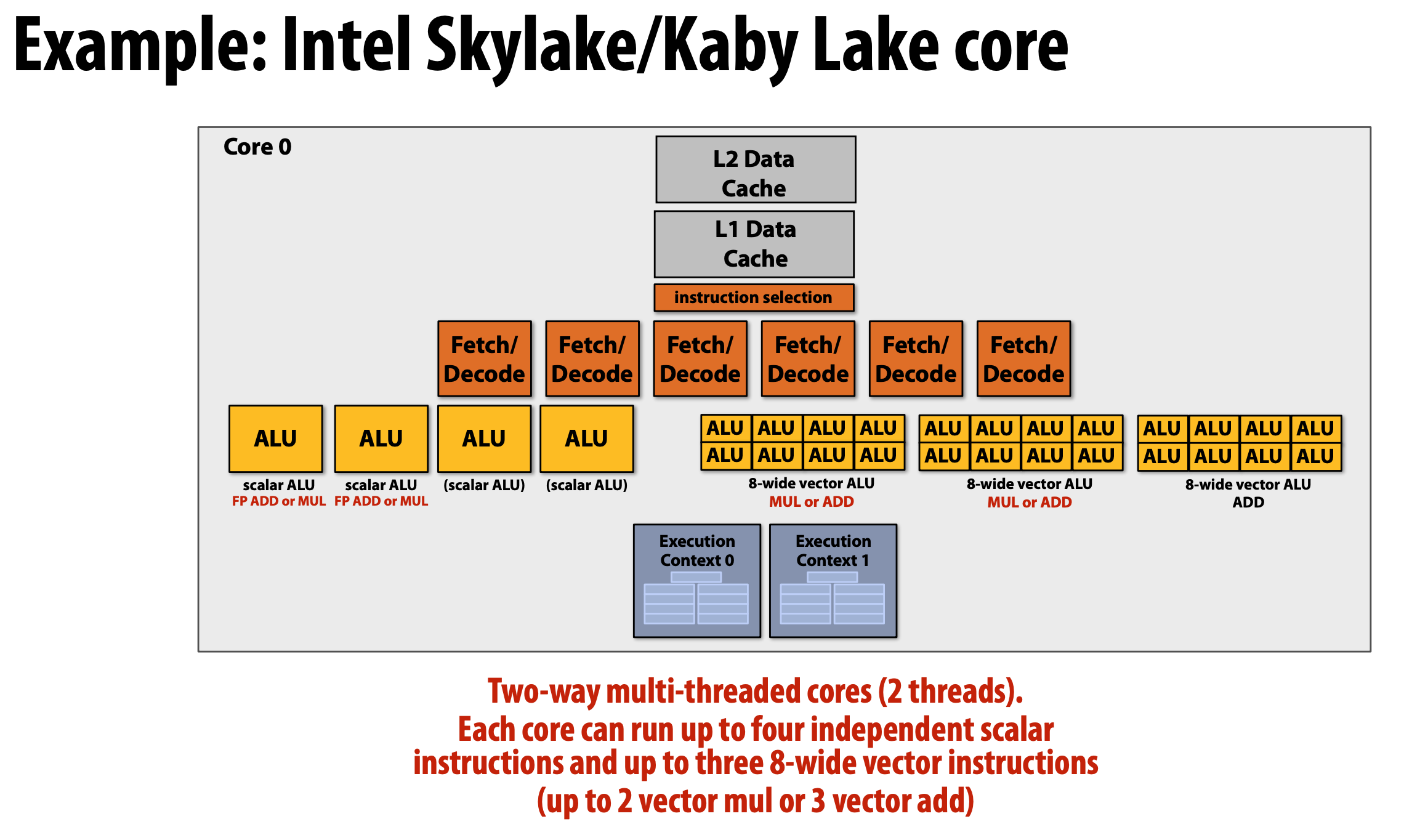
Example: Intel Skylake
Exercises
Ex - 1: SIMD
uint64_t a = 0, b = 0;
int steps = INT_MAX;
for (int i = 0; i < steps; i++) { a++; b++; }
for (int i = 0; i < steps; i++) { a++; a++; }
Regardless of compilation optimization, which loop is faster?
- The 1st one is faster because of SIMD optimization within CPU.
Ex - 2: Cache False Sharing
int *a = new int[1024];
void worker(int idx)
{
    for (int j = 0; j < 1e9; j++)
        a[idx] = a[idx] + 1;
}
Suppose there are two programs:
- P1: Four threads to execute
worker(0), worker(1), worker(2), worker(3). - P2: Four threads to execute
work(0), worker(16), worker(32), worker(64). - For both of them, four threads is running on different cores.
Which one is faster?
- The 2nd one is faster.
- On most machines, the size of one cache-line is 64 bytes.
- For program P1,
a[0, 1, 2, 3]will be in same one L3-cache-line. Since L1-cache is exclusive for each core, once the same cache-line is modified, the MESI protocol will cause multiple "cache-line write back" (from L1, write back to L3).- This is called "Cache False Sharing", i.e. two processors write to different addresses, but addresses map to the same cache line.
- For program P2,
a[0], a[16], a[32], a[64], their gap is 64 bytes, hence they will be not in same cache-line. There is no cache-line-write-back during the loop.
Another classic cache issue is "Cache Ping Pong", i.e. multi-threads write one same variable.
Ex - 3: CPU Cores and Threads
Suppose there are 1 CPU with 4 cores on my machine, we wirte some prorgams to implement multi-threads sorting.
- P1: 4 threads
- P2: 8 threads
P1 is faster than P2, since there is no context-switching in P1. Is it right?
- Obviously not. We need to consider how many thread one core can run. If one core can run two threads (i.e. there are two set of registers in one core), then P2 has no context-switching, too.
- Code implementation is also relevant. Superscalar-friendly and cache-friendly code is better.


