stm32用spi开发W25Q128(Flash闪存芯片)
前提提要spi概念
目录
stm32用spi开发W25Q128(Flash闪存芯片)
开发流程
1. 看硬件数据手册,确定通信协议,时序图,引脚
2. 初始化要用引脚
W25Q128(Flash闪存芯片)介绍
串行Flash芯片,型号是W25Q128,容量是128Mbit,该存储IC采用SPI接口进行通信。
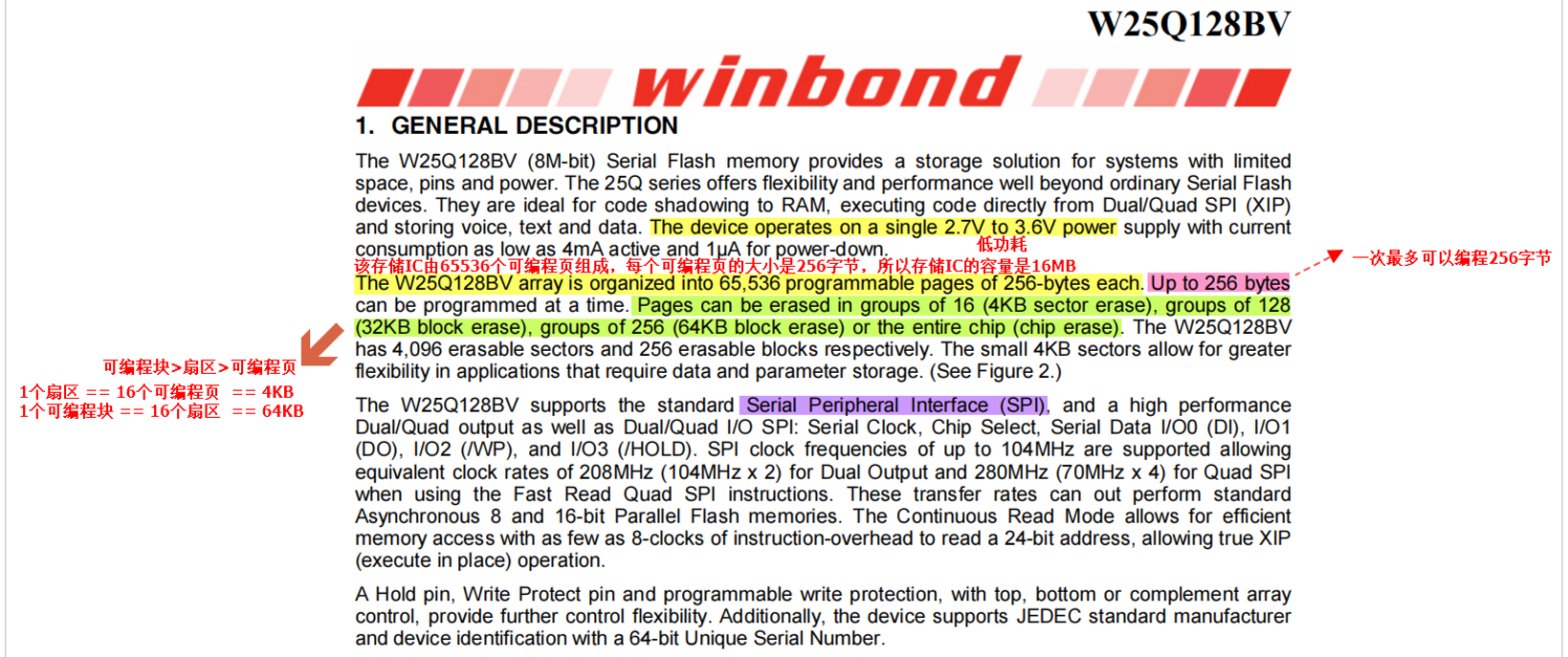
* 可编程块>扇区>可编程页
* 1个扇区 == 16个可编程页== 4KB
* 1个可编程块 == 16个扇区==64KB
* 该存储IC由65536个可编程页组成,每个可编程页的大小是256字节,所以存储IC的容量是16MB
* 一次最多可以编程256字节
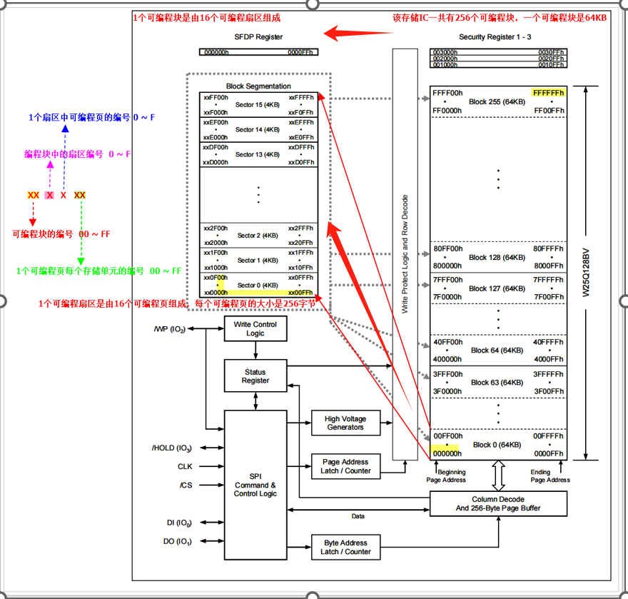
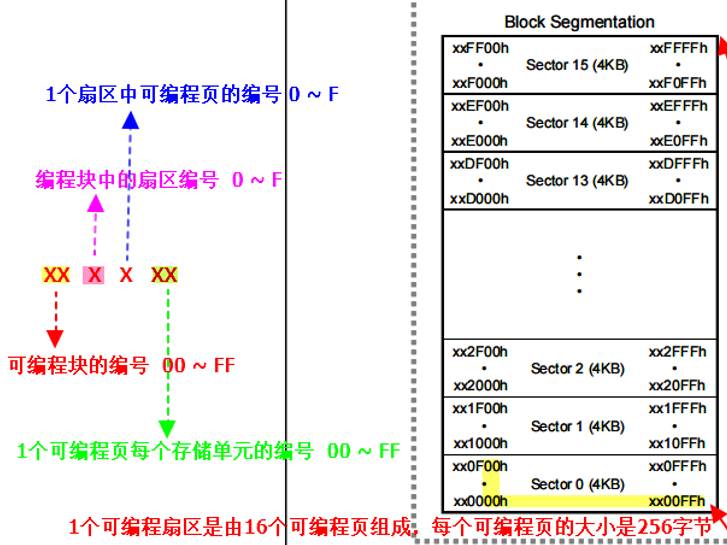
内存分布
1个可编程块是由16个可编程扇区组成
该存储IC一共有256个可编程块,一个可编程块是64KB
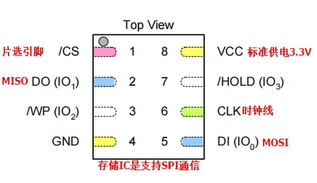
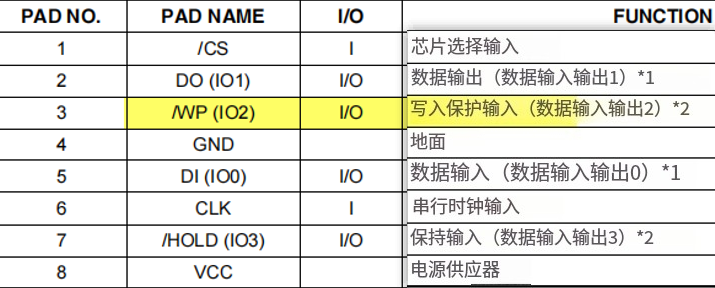
引脚说明
指令介绍
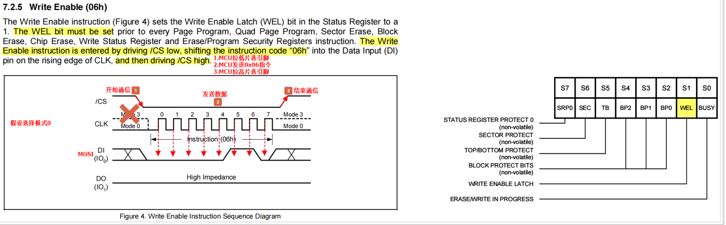
(1) 写使能指令 0x06
折叠重要但又不重要的图片
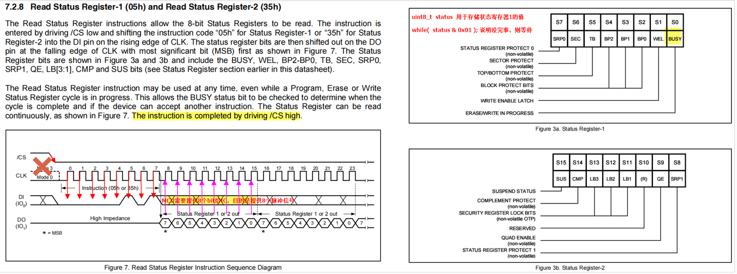
(2) 读状态寄存器 0x35
折叠重要但又不重要的图片
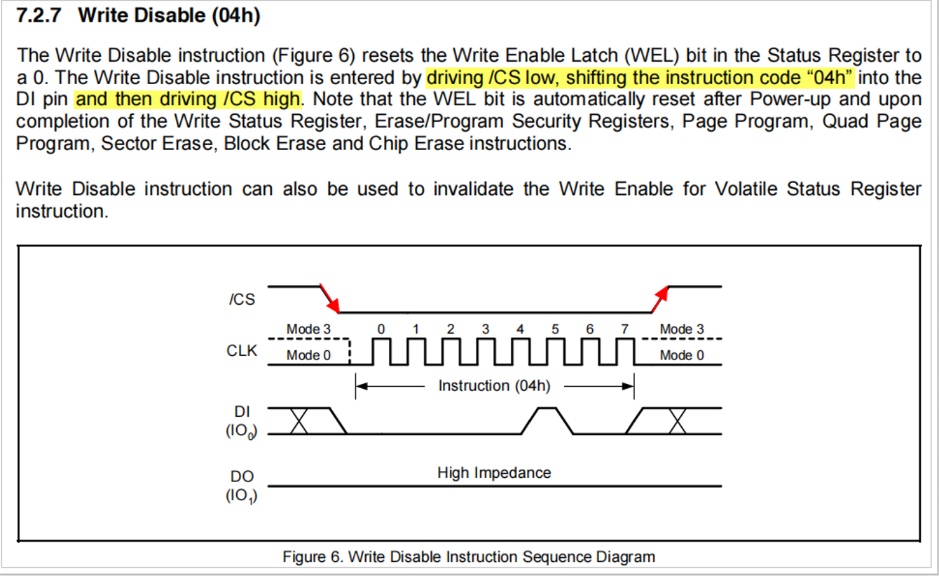
(3) 写失能指令 0x04
折叠重要但又不重要的图片
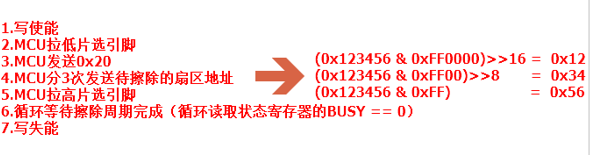
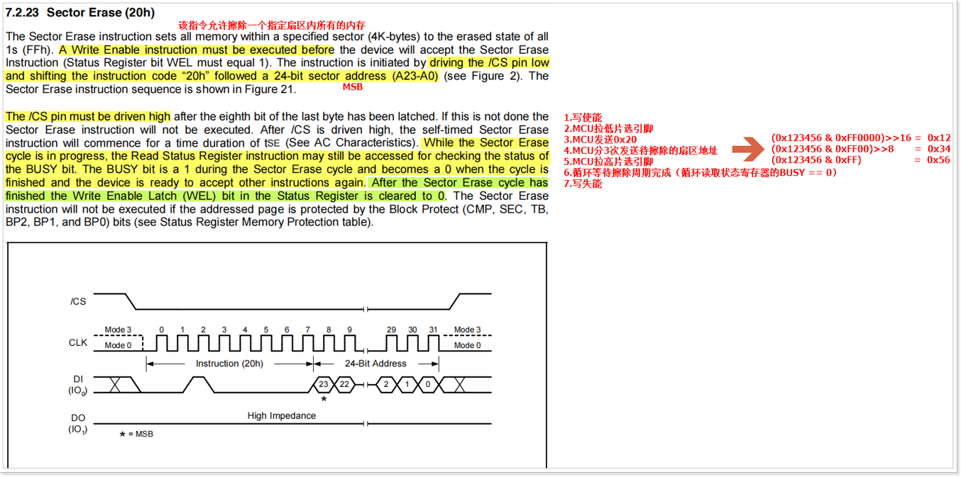
(4) 擦除扇区指令 0x20
折叠重要但又不重要的图片
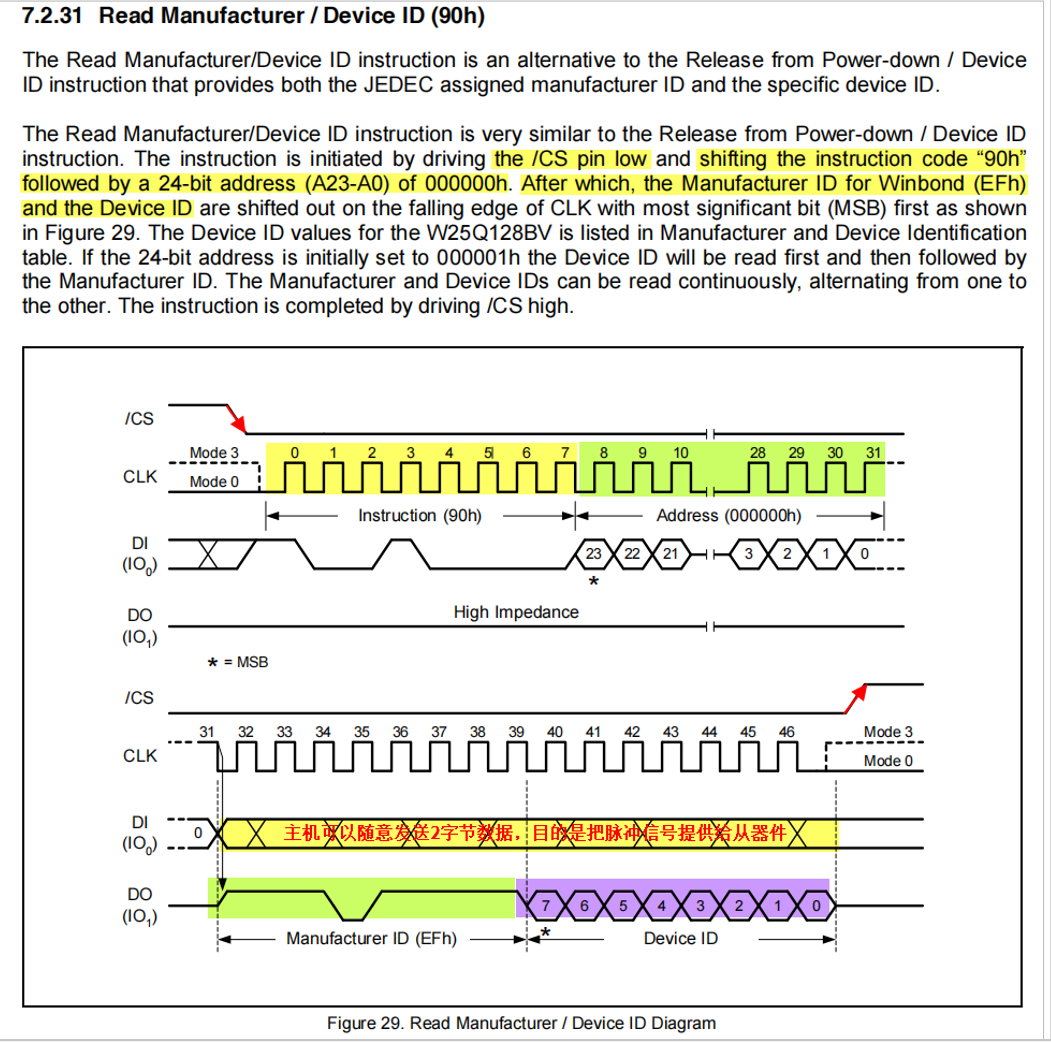
(5) 读取厂商和设备ID 0x90
折叠重要但又不重要的图片
读状态寄存器1 0x05
读取数据 0x03
页编辑 0x02
代码
折叠重要但又不重要的图片
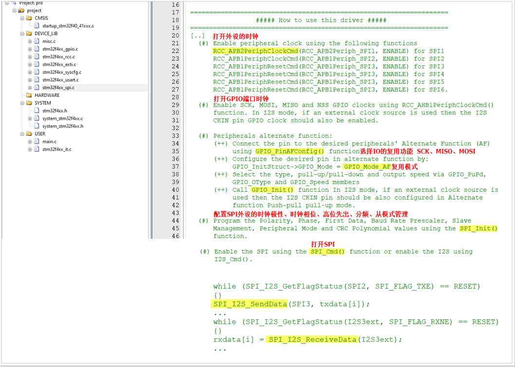
点击查看spi硬件初始化代码
void W25Q128_Config(void)
{
  SPI_InitTypeDef  SPI_InitStructure;
  GPIO_InitTypeDef GPIO_InitStructure;

  //打开SPI1的时钟
  RCC_APB2PeriphClockCmd(RCC_APB2Periph_SPI1, ENABLE);

  //打开GPIOB端口的时钟
  RCC_AHB1PeriphClockCmd(RCC_AHB1Periph_GPIOB,ENABLE);

  //选择IO口的复用功能
  GPIO_PinAFConfig(GPIOB, GPIO_PinSource3, GPIO_AF_SPI1);		//SCK
  GPIO_PinAFConfig(GPIOB, GPIO_PinSource4, GPIO_AF_SPI1);		//MISO
  GPIO_PinAFConfig(GPIOB, GPIO_PinSource5, GPIO_AF_SPI1);     	//MOSI

  GPIO_InitStructure.GPIO_Mode 	= GPIO_Mode_AF;					//复用模式
  GPIO_InitStructure.GPIO_Speed = GPIO_Speed_50MHz;
  GPIO_InitStructure.GPIO_OType = GPIO_OType_PP;
  GPIO_InitStructure.GPIO_PuPd  = GPIO_PuPd_DOWN;
  GPIO_InitStructure.GPIO_Pin 	= GPIO_Pin_3|GPIO_Pin_4|GPIO_Pin_5;
  GPIO_Init(GPIOB, &GPIO_InitStructure);

  //配置CS片选引脚  输出模式
  GPIO_InitStructure.GPIO_Pin 	= GPIO_Pin_14;
  GPIO_InitStructure.GPIO_Mode 	= GPIO_Mode_OUT;
  GPIO_InitStructure.GPIO_OType = GPIO_OType_PP;
  GPIO_InitStructure.GPIO_Speed = GPIO_Speed_50MHz;
  GPIO_InitStructure.GPIO_PuPd 	= GPIO_PuPd_NOPULL;
  GPIO_Init(GPIOB, &GPIO_InitStructure);

  //片选引脚,空闲状态为高电平
  W25Q128_CS(1);

  //配置SPI1  W25Q128存储IC支持模式0和模式3
  SPI_InitStructure.SPI_Direction = SPI_Direction_2Lines_FullDuplex;	//全双工
  SPI_InitStructure.SPI_Mode = SPI_Mode_Master;							//主模式
  SPI_InitStructure.SPI_DataSize = SPI_DataSize_8b;						//8bit数据位
  SPI_InitStructure.SPI_CPOL = SPI_CPOL_High;							//时钟极性  1
  SPI_InitStructure.SPI_CPHA = SPI_CPHA_2Edge;							//时钟相位  1    11 --模式3
  SPI_InitStructure.SPI_NSS = SPI_NSS_Soft;								//软件控制CS片选
  SPI_InitStructure.SPI_BaudRatePrescaler = SPI_BaudRatePrescaler_4;

  SPI_InitStructure.SPI_FirstBit = SPI_FirstBit_MSB;					//高位先出
  SPI_Init(SPI1, &SPI_InitStructure);

  //使能SPI1
  SPI_Cmd(SPI1, ENABLE);

}
点击查看用读取W25Q128官方id代码
//发送一个字节,并且会得到一个字节
uint8_t W25Q128_SendByte(uint8_t byte)
{
  /*!< Loop while DR register in not emplty */
  while (SPI_I2S_GetFlagStatus(SPI1, SPI_I2S_FLAG_TXE) == RESET);

  /*!< Send byte through the SPI1 peripheral */
  SPI_I2S_SendData(SPI1, byte);

  /*!< Wait to receive a byte */
  while (SPI_I2S_GetFlagStatus(SPI1, SPI_I2S_FLAG_RXNE) == RESET);

  /*!< Return the byte read from the SPI bus */
  return SPI_I2S_ReceiveData(SPI1);
}


//读取设备ID   0x17
uint8_t W25Q128_ReadDeviceID(void)
{
	uint8_t device_id = 0;

	//1.把片选引脚拉低
	W25Q128_CS(0);

	//2.MCU发送指令  0x90
	W25Q128_SendByte(0x90);

	//3.MCU发送地址
	W25Q128_SendByte(0x00);
	W25Q128_SendByte(0x00);
	W25Q128_SendByte(0x00);

	//4.MCU提供脉冲,得到厂商ID
	W25Q128_SendByte(0xFF);

	//5.MCU提供脉冲,得到设备ID
	device_id = W25Q128_SendByte(0xFF);

	//6.把片选引脚拉高
	W25Q128_CS(1);

	return device_id;
}


int main()
{
	uint8_t buf[128] = {0};

	//1.硬件的初始化
	USART1_Config(9600);
	W25Q128_Config();

	//2.读取W25Q128的设备ID
	sprintf((char *)buf,"Device ID = %#X\r\n",W25Q128_ReadDeviceID());
	USART1_SendString((char *)buf);

	while(1)
	{

	}
}
点击查看W25Q128存储,查看代码
//擦除扇区
void sFLASH_EraseSector(uint32_t SectorAddr)
{
  /*!< Send write enable instruction */
  sFLASH_WriteEnable();

  /*!< Sector Erase */
  /*!< Select the FLASH: Chip Select low */
  sFLASH_CS_LOW();
  /*!< Send Sector Erase instruction */
  sFLASH_SendByte(0x20);
  /*!< Send SectorAddr high nibble address byte */
  sFLASH_SendByte((SectorAddr & 0xFF0000) >> 16);
  /*!< Send SectorAddr medium nibble address byte */
  sFLASH_SendByte((SectorAddr & 0xFF00) >> 8);
  /*!< Send SectorAddr low nibble address byte */
  sFLASH_SendByte(SectorAddr & 0xFF);
  /*!< Deselect the FLASH: Chip Select high */
  sFLASH_CS_HIGH();


  //7.发送写失能指令
  sFLASH_WaitForWriteEnd();
  /*!< Wait the end of Flash writing */
  sFLASH_WaitForWriteEnd();
}


//页写入
/*
* @brief写一个以上的字节到FLASH与一个单一的写周期
*(页写顺序)。
* @注意字节数不能超过FLASH页面大小。
* @param  pBuffer:指向包含要写入数据的缓冲区的指针
*到FLASH。
* @param  WriteAddr: FLASH写入的内部地址。
* @param  NumByteToWrite:写入FLASH的字节数,必须相等
*或小于"sFLASH_PAGESIZE"值。
* @retval  无
*/
void sFLASH_WritePage(uint8_t* pBuffer, uint32_t WriteAddr, uint16_t NumByteToWrite)
{
  /*!< Enable the write access to the FLASH */
  sFLASH_WriteEnable();

  /*!< Select the FLASH: Chip Select low */
  sFLASH_CS_LOW();
  /*!< Send "Write to Memory " instruction */
  sFLASH_SendByte(0x02);
  /*!< Send WriteAddr high nibble address byte to write to */
  sFLASH_SendByte((WriteAddr & 0xFF0000) >> 16);
  /*!< Send WriteAddr medium nibble address byte to write to */
  sFLASH_SendByte((WriteAddr & 0xFF00) >> 8);
  /*!< Send WriteAddr low nibble address byte to write to */
  sFLASH_SendByte(WriteAddr & 0xFF);

  /*!< while there is data to be written on the FLASH */
  while (NumByteToWrite--)
  {
    /*!< Send the current byte */
    sFLASH_SendByte(*pBuffer);
    /*!< Point on the next byte to be written */
    pBuffer++;
  }

  /*!< Deselect the FLASH: Chip Select high */
  sFLASH_CS_HIGH();

  /*!< Wait the end of Flash writing */
  sFLASH_WaitForWriteEnd();
}


/**
  * @brief  Reads a block of data from the FLASH.
  * @param  pBuffer: pointer to the buffer that receives the data read from the FLASH.
  * @param  ReadAddr: FLASH's internal address to read from.
  * @param  NumByteToRead: number of bytes to read from the FLASH.
  * @retval None
  */
void sFLASH_ReadBuffer(uint8_t* pBuffer, uint32_t ReadAddr, uint16_t NumByteToRead)
{
  /*!< Select the FLASH: Chip Select low */
  sFLASH_CS_LOW();

  /*!< Send "Read from Memory " instruction */
  sFLASH_SendByte(0x03);

  /*!< Send ReadAddr high nibble address byte to read from */
  sFLASH_SendByte((ReadAddr & 0xFF0000) >> 16);
  /*!< Send ReadAddr medium nibble address byte to read from */
  sFLASH_SendByte((ReadAddr& 0xFF00) >> 8);
  /*!< Send ReadAddr low nibble address byte to read from */
  sFLASH_SendByte(ReadAddr & 0xFF);

  while (NumByteToRead--) /*!< while there is data to be read */
  {
    /*!< Read a byte from the FLASH */
    *pBuffer = sFLASH_SendByte(0xA5);
    /*!< Point to the next location where the byte read will be saved */
    pBuffer++;
  }

  /*!< Deselect the FLASH: Chip Select high */
  sFLASH_CS_HIGH();
}


int main()
{
	uint8_t readbuf[11] = {0};

	USART1_Config(9600);
	W25Q128_Config();
	//2.擦除一个扇区  0x 00  0  0  00
	sFLASH_EraseSector(0x000000);

	//3.向擦除的扇区中的第0页写入数据
	sFLASH_WritePage("hello world",0x000000,11);

	//4.从存储IC的指定地址下读取数据
	sFLASH_ReadBuffer(readbuf,0x000000,11);

	//5.输出读取的数据
	USART1_SendString((char *)readbuf);

	while(1)
	{
		delay_ms(100);
		//printf("%s\r\n",(char *)W25Q128_ReadDeviceID);
	}

}
点击查看模拟spi代码
修改方面:端口模式改了,删掉硬件spi初始化,重写数据传输即可
重要:模拟spi可以看上篇文章,主要是将端口初始化修改还有传输数据修改即可
注意:大方面可以根据stm32官方的例程修改,例如端口,时钟之类的,但是小的方面要根据W25Q128官方的芯片手册的要求修改,例如命令的不同,传输命令的时序图不同,要注意
点击查看好用的宏代码
#define sFLASH_CS_LOW()       GPIO_ResetBits(GPIOB, GPIO_Pin_14)
#define sFLASH_CS_HIGH()      GPIO_SetBits(GPIOB, GPIO_Pin_14)

#define  W25Q128_SCK(n)  	(n) ? GPIO_SetBits(GPIOB,GPIO_Pin_3)  : GPIO_ResetBits(GPIOB,GPIO_Pin_3)
#define  W25Q128_MOSI(n)  (n) ? GPIO_SetBits(GPIOB,GPIO_Pin_5)  : GPIO_ResetBits(GPIOB,GPIO_Pin_5)
#define  W25Q128_MISO		   GPIO_ReadInputDataBit(GPIOB, GPIO_Pin_4)
#define  W25Q128_CS(n)    (n) ? GPIO_SetBits(GPIOB,GPIO_Pin_14) : GPIO_ResetBits(GPIOB,GPIO_Pin_14)
点击查看模拟spi模式3,模式0的代码
小插曲:模拟spi写的时候逻辑没问题,但死活不行,排查了很久,才发现把cs当成SCK了


//发送一个字节,并且会得到一个字节    假设采用模式3   SCK引脚空闲高电平,第二个边沿锁存数据
//uint8_t W25Q128_SendByte(uint8_t byte)
//{
//	int i = 0;
//	uint8_t data = 0;
//
//	 //1.SCK引脚输出高电平
//	 W25Q128_SCK(1);
//	 delay_us(5);
//
//	 //3.循环发送8次,每次发送一个bit  遵循MSB 高位先出
//	 for(i=0;i<8;i++)
//	 {
//		  //2.SCK引脚输出低电平,此时第一个边沿出现
//			W25Q128_SCK(0);
//			delay_us(5);
//
//		 //4.判断待发送的字节的最高位  ???? ???? & 1000 0000
//		 if( byte & 0x80 )
//		 {
//				W25Q128_MOSI(1);
//		 }
//		 else
//				W25Q128_MOSI(0);
//
//		 byte <<= 1;
//		 delay_us(5);
//
//		 //5.SCK引脚输出高电平,此时第二个边沿出现
//		 W25Q128_SCK(1);
//		 delay_us(5);
//
//		 //6.此时从机会响应一个bit,主机需要接收!
//		 data <<= 1;
//		 data |= W25Q128_MISO;
//		 delay_us(5);
//	 }
//
//	 return data;
//}

//发送一个字节,并且会得到一个字节 模式0
uint8_t W25Q128_SendByte(uint8_t byte)
{
	int i=0;
	uint8_t data=0;

	//第一步,确保SCK低电平
	W25Q128_SCK(0);
	delay_us(5);

	for(i=0;i<8;i++)
	{
		if( byte & 0x80)
		{
		W25Q128_MOSI(1);
		}
		else
		W25Q128_MOSI(0);

		byte <<= 1;
		delay_us(5);

		W25Q128_SCK(1);
		delay_us(5);


		data <<= 1;
		data |=W25Q128_MISO;
		delay_us(5);

		W25Q128_SCK(0);
		delay_us(5);

	}
	return data;

}
参考李明轩老师笔记


【推荐】国内首个AI IDE,深度理解中文开发场景,立即下载体验Trae
【推荐】编程新体验,更懂你的AI,立即体验豆包MarsCode编程助手
【推荐】抖音旗下AI助手豆包,你的智能百科全书,全免费不限次数
【推荐】轻量又高性能的 SSH 工具 IShell:AI 加持,快人一步
· 阿里最新开源QwQ-32B,效果媲美deepseek-r1满血版,部署成本又又又降低了!
· 开源Multi-agent AI智能体框架aevatar.ai,欢迎大家贡献代码
· Manus重磅发布:全球首款通用AI代理技术深度解析与实战指南
· 被坑几百块钱后,我竟然真的恢复了删除的微信聊天记录!
· AI技术革命,工作效率10个最佳AI工具