DAC Essentials
http://e2e.ti.com/blogs_/b/analogwire/archive/tags/DAC%2bEssentials
DAC Essentials: A new blog series
A digital-to-analog converter, or DAC, performs the opposite function of an analog-to-digital converter, or ADC. Duh, right? But, have you ever wondered exactly what’s going on inside that integrated circuit? Unlike other analog components, DACs are much less familiar to many engineers.
This is the first post in a new blog series from me and my buddy Tony Calabria on Analog Wire. A few times a month we’ll be discussing precision DAC specifications from the ground up. We’ll explain architectural differences, the key specifications, calibration and deglitching techniques, reference and output buffer circuitry, and application specific concerns.
On the surface, DACs may seem limited to only a few applications. For many designers, a DAC brings to mind AC signal generation or the legacy of Burr-Brown audio DACs.
While DACs are a common component in audio equipment (something’s gotta convert your MP3 collection to vibrations in your headphones, right?), they’re also found in the DC application space. In addition to audio, you’ll find DACs in wireless base stations, medical instrumentation, industrial communication, biasing networks, process control, and more. Some DACs are even used to calibrate other DACs and some are found inside SAR and delta-sigma ADCs!

Many DAC architectures are simply networks of resistors and switches, or tap points, to generate specific voltages or currents. Some architectures are a little more complex and use delta-sigma bit-streams or current-steering toplogies to achieve strong AC specs and high-speed throughput. An output buffer is sometimes included on silicon to isolate the DAC from its load, and some architectures assume that a buffer will be provided external to the IC.
Because of process and price limitations in discrete components, DACs are primarily created as integrated circuits. On silicon resistor ratios can be more tightly controlled and offered at much lower prices than discrete solutions, while bringing many integrated features to the table. In the precision DAC space, we see variability across several critical parameters, including:
- Resolution
- Channel count
- Update rate
- Digital interface
- Current and/or voltage outputs
- Glitch energy & settling time
- Zero-code error
- Offset & gain error
- Linearity (INL/DNL)
- Peripheral features (GPIOs, Alarms, etc)
In our next post in this series, we’ll explore the ideal DAC to establish the most basic fundamentals. After that, we'll delve into the two primary DAC architectures: the string DAC and R-2R DAC. Be sure to check back every few weeks or subscribe to Analog Wire so you don't miss out!
Leave your comments in the section below if you’d like to hear more about anything I mentioned in this post, or if there’s a topic you’d like me or Tony to address in future posts. We’d love to hear from you!
PS: You can click this link read the other posts in the DAC Essentials series.
DAC Essentials: The pursuit of perfection
In my last post, I introduced the DAC Essentials blog series here on Analog Wire. If you missed it, check it out here.
While most IC designers I know would shudder to think of a datasheet this way, the purpose of a datasheet is typically to explain how a device deviates from its ideal model. If it were possible for semiconductor suppliers to design and manufacture perfect, ideal operational amplifiers, for instance, we wouldn’t need op amp datasheets because everyone would know that they have very specific properties (infinite open-loop gain, infinite input impedance, etc). If only it were that simple.
Tony and I wanted to begin this blog series with a brief tutorial explaining the properties of an ideal DAC (digital-to-analog converter) before delving into its more complex specifications. The figure below illustrates the ideal DAC transfer function and highlights the parameters we’ll discuss.
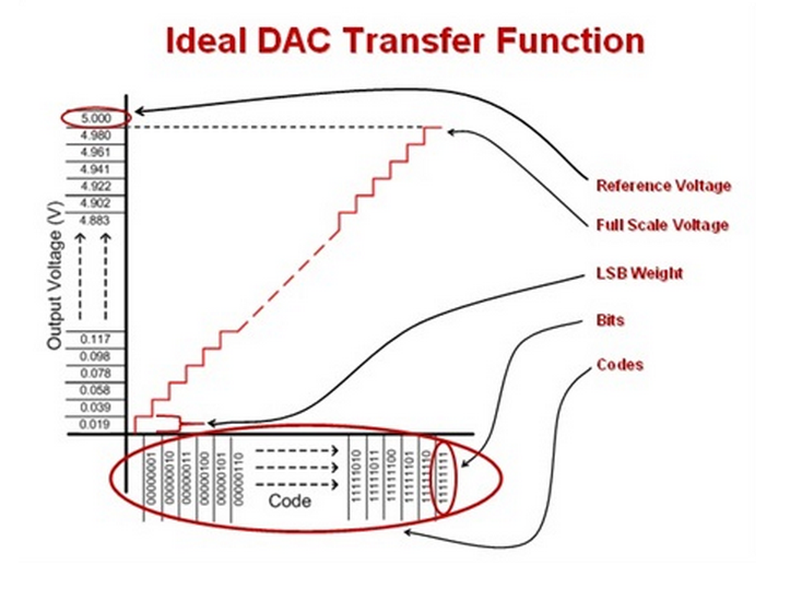
The most fundamental property of any data converter, whether DAC or ADC (analog-to-digital converter), is its resolution. For a DAC, resolution describes the number of bits available in the digital domain to represent the analog output signal. With the resolution, we can calculate the number of codes, or total number of possible outputs, that we can write to the converter.

The reference voltage applied to a data converter, whether internal or external, is very important. Any converter is only as good as its reference, as any noise or drift from the reference will be seen at the output. Note that we’ll address reference considerations in a future post, so stay tuned for more on that topic.
For a DAC, the reference voltage sets the output range and step size from code to code. Output step size from code to code is usually described as “least significant bit weight” or LSB weight. With the number of codes and reference voltage, we can calculate LSB weight as shown below. In an ideal DAC, every code-to-code transition is separated by exactly 1 LSB.

It’s a little tricky to consider, but with n bits, the highest number we can actually count to is 2n – 1. If that leaves you scratching your head, consider the 2 bit case. With 2 bits, we can count 0, 1, 2, and 3 – but not 4 (24). This digital behavior is also consistent with the internal analog structure of most DACs, but we’ll get into that with a later post as well... have I convinced you to subscribe to the series yet? For now, take it on faith that the full-scale output range of a DAC can be calculated as shown below.

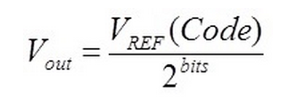
Finally, we can define the ideal DAC transfer function as:
Here are the key properties of the ideal DAC to remember:
- Near rail-to-rail output set by the reference input, remember the full scale output should be Vref - 1 LSB
- Any two sequential codes are exactly 1 LSB apart
- No missing codes, fully monotonic
- Instantaneous transition from code-to-code
In our next post, I’ll explain how real DACs deviate from the ideal DAC by discussing the static specifications used to describe linearity.
Leave your comments in the section below if you’d like to hear more about anything mentioned in this post, or if there is a topic you would like to see included in future posts!
DAC Essentials: String theory
No, I'm not actually going to talk about particle physics today - though that would be cool...instead we'll be discussing the theory of the string DAC architecture. String theory!
The string DAC, sometimes referred to as the Kelvin divider or Kelvin-Varley divider after its inventors, is one of the most straightforward methods used to design a DAC. In its simplest form, the string DAC is just a series of equally sized resistors with a tap point between each resistor. Based on the digital code applied to the DAC, the appropriate tap point will be switched to the output buffer. This limited switch movement results in very low glitch energy, which my buddy Tony Calabria will delve into in a future post in this series. Ideally, each resistor will induce a voltage drop from the reference equal to 1 LSB. A simplified illustration of the architecture is shown below.

As resolution increases in the string DAC, the number of resistors required for the design increases exponentially. A n-bit string DAC requires 2n resistors, so in general a high-resolution string DAC would require a large IC package. That translates to 65,536 resistors for a 16-bit DAC, 262,144 for 18-bits, and 1,048,576 resistors for 20-bits! Cascaded segmentation techniques are sometimes used to reduce the number of resistors required, but for our purposes we will not consider segmentation, as architectural trends tend to hold true at the application level even if segmentation was implemented.
The accuracy of each resistor value directly determines linearity. If any resistor in the string isn’t the appropriate value, we’ll see poor differential non-linearity (DNL) at the code transition corresponding to that resistor. Also, the integral non-linearity (INL) of all subsequent codes would also be offset by the mismatch. Given the number of resistors in a typical string DAC design, it’s impractical to trim every resistor and as a result, we typically accept DNL errors to some extent. However, it is still highly desirable to maintain good INL so sectionalized trimming on groups of resistors is frequently implemented to overcome trimming every resistor, which presents itself as a “staircase” effect on the INL graph shown below.

A perk of the string DAC is that the input impedance looking in from the reference input remains constant except during instantaneous code transitions. Other data converter architectures, especially SAR ADCs, have dynamic loading conditions that make a reference buffer a requirement, while the string DAC is more forgiving. In general, however, it’s a good idea to buffer any reference – especially if the input/output will change with great frequency. It’s also important to note that the equivalent input impedance from the reference is typically very high, making most string DACs very power efficient.
The final and most subtle element of the string DAC design is the divider present before the string resistors and tap points. This resistor is equal to the equivalent impedance of the rest of the resistors in the string and effectively halves the reference input. This is done in an effort to lower the common mode input requirements of the output buffer and help keep the cost low while delivering good performance. To compensate for this, the output buffer is typically in a non-inverting gain of 2 configuration, though sometimes the feedback resistor can be digitally controlled to realize different gains.
A few things to remember about string DACs:
- Low cost via simplicity of design
- Low glitch energy
- Inherent monotonicity
- Low power consumption
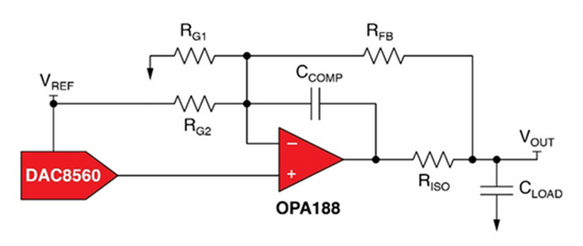
The string DAC frequently finds a home in portable battery powered applications that can make great use of its low power consumption. Additionally the string DAC is used in applications like closed loop control systems that leverage its inherent monotonicity and in low-cost applications where the DAC is providing some calibration feature to a system, rather than being the ‘star’ of the show as we may see in other DAC applications. If a string DAC sounds like something that interests you be sure to check out a few TI string DACs such as: DAC8562, DAC8560, DAC8568, DAC7678, DAC8411, DAC8718, orDAC8728.
If you liked this, be sure to check out our other posts in the DAC Essentials series.
DAC Essentials: How accurate is your DAC?
We’ve covered a lot of material in the DAC Essentials series, starting with a simple ideal digital-to-analog converter (DAC) all the way to complex problems, like reducing glitch. In this final post in the series, we’ll talk about total unadjusted error (TUE).
Precision DACs deliver excellent DC, or very low frequency, performance. In many precision DAC applications, the AC error specifications related to code transitions, glitch and slew rate, are negligible when defining the accuracy of the DAC. This is because the output will spend a majority of its time settled and unchanging.
In my “DAC Essentials: Static specifications & linearity” post, I explained all of the DAC DC error parameters: offset error, zero code error, gain error, differential non-linearity (DNL) and integral non-linearity (INL). When trying to express how accurate a DAC is at DC, it’s challenging to keep all of those error sources in mind. That’s the beauty of TUE. It gives you a single number that succinctly explains how accurate the DC DAC output is as a result of the sum of all of these error sources. The only catch is you have to do a little statistics.
In statistics, a technique called RSS, or root sum squared, is used to sum uncorrelated error sources for error analysis. With string and ladder DAC architectures, offset, gain and INL error come from different components of the DAC architecture. This means they’re uncorrelated, and the RSS technique is safe to apply. Here’s the equation:

You may have noticed that I didn’t include zero code error and DNL. That’s because zero code error only applies to a very small portion of the DAC output. For a 16-bit DAC, this might be a few hundred codes out of 65,536 total codes. DNL, meanwhile, is actually included in the error calculation via INL.
Now let’s go through a short example that shows how to calculate TUE. Below are the datasheet maximum and typical specifications for the 16-bit, two-channel DAC8562.

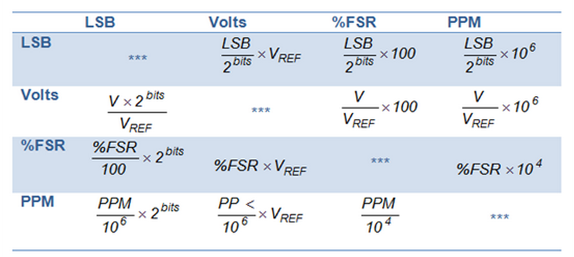
Each of the specifications for the DAC8562 are provided in different units, which is typical across the industry. To calculate TUE, everything needs to be in the same unit, so we’ll use the table below to convert the values.
Once we’ve converted units, we can plug the values back into the TUE equation and calculate the total unadjusted error for the DAC8562.
Using the maximum values for all of the specifications provides what I refer to as the “probable maximum TUE” of +/-111 LSBs, +/-8.5mV, or 0.17% FSR. I say this because the max values in the datasheet are three-sigma figures that should encompass 99.7% of all parts ever produced. On a typical Gaussian distribution, these edge cases are not likely to happen. You’re even less likely to find a part that actually displays the maximum errors for all parameters (an “absolute maximum error” so to speak - the figure you would see from simply summing all of the errors together). Even this probable maximum TUE is a somewhat unlikely unit to observe.
Using the typical figures provides the most realistic estimation of what you’ll see from most systems. The typical TUE for the DAC8562 is +/- 23 LSBs, 1.78mV, or 0.0356% FSR. Check out this TI Precision Design to see this method in practice, and proven reliable, with real data on a real system.
Remember that these parameters also have direction associated with them. For a DAC with positive offset error, negative gain error would actually help make the system more accurate. This isn’t taken into account when you use RSS to sum the maximum errors. So in many cases, RSS on typical error figures still provides a pretty modest estimate of TUE.
While this post marks the end of the DAC Essentials series, you’ll find me blogging on other topics on The Hub, our blog focused exclusively on precision analog tips, tricks and design techniques.
And be sure to check out my new Engineer It video if you want to get some advice on how to select the perfect DAC for your system.
As always, leave your comments below if you’d like to hear more about anything mentioned in this post, or if there is something you would like to see included in a future post here or on The Hub.
DAC Essentials: The resistor ladder
In my last post, I discussed the string DAC architecture and its tendencies― if you missed it you can view that post here. This post will focus on two very similar architectures, the R-2R DAC and the MDAC.
Recall that the big limitation of the string DAC is the challenge associated with realizing a high resolution design and maintaining linearity. The number of resistors required for the string DAC increases exponentially as resolution increases, unless clever design tricks are implemented like cascaded resistor strings or interpolating amplifiers. The R-2R architecture directly addresses this problem by utilizing a binary weighted resistor ladder structure, illustrated below:

Each bit of resolution of the DAC is made of one set of R resistor, 2R resistor, and 1 switch that moves between the reference voltage and ground creating a voltage divider at the output node. Typically there is an on-silicon output buffer included. If you’re having a hard time understanding how the binary weighted divider works, I recommend creating this circuit in TINA-TI where you can simulate each switch position.
The R-2R DAC sees a variable impedance at the reference node, so a reference buffer is a requirement for applications where the DAC output is going to be changed very frequently in order to keep reference settling time from impacting DAC output settling time. Usually this buffer is included on silicon, just like the output buffer, but make sure you consult your device’s datasheet before making any assumptions.
The MDAC, or multiplying DAC, uses a very similar topology – the same R-2R ladder in fact – except that the position of the reference input node and the output node are swapped. This change makes the R-2R ladder a current divider rather than a voltage divider. Because of this a transimpedance output stage is required to convert from current output to voltage output. Typically this buffer is not included on silicon but the feed-back resistor required for the transimpedance stage is included. Featuring the feedback resistor on silicon helps to ensure resistor matching to the rest of the R-2R ladder in terms of both value and drift behavior.
Not including an output buffer may seem like a disadvantage to the MDAC but in many ways it is actually quite helpful. Moving the amplifier to outside the device allows for great flexibility in design, applications with relaxed requirements can choose cheaper amplifiers and save money versus the price of a fully integrated solution. Meanwhile, in high-performance systems it is beneficial to utilize discrete amplifiers that are made on strong pure-analog processes.
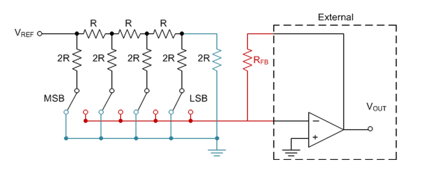
As far as performance tendencies go, the R-2R and MDAC architectures have very similar properties and we’ll discuss them simultaneously.
Since there are fewer resistors in these designs we can implement a much more comprehensive trimming scheme to achieve very strong linearity. Trimming circuits also take up space, though, so the R-2R and MDAC packages tend to be larger than the string DAC.
The number of switches moving in the R-2R and MDAC designs is code-dependent. In some cases, every switch of the DAC may have to move to increment to the next code which will create much higher glitch energy than the string DACs.
Some things to remember about the R-2R DAC and MDAC:
- Excellent INL/DNL
- Medium to high glitch energy
- Larger packages
The R-2R and MDACs find homes in virtually any application that is very high performance. That includes industrial programmable logic controllers, automated test and measurement equipment, precision instrumentation, and various other applications. Since the MDAC does not feature reference or output buffers it can deliver good results in medium speed applications as well such as waveform generation or AC attenuators. If these devices are of interest to you be sure to check out a few TI R-2R DACs and MDACs such as: DAC8811, DAC8822, DAC8734, DAC9881, DAC8881, or DAC7654.
This post finishes out the discussion of the DAC basics. Tony Calabria will continue the DAC Essentials series with a deep dive into glitch and glitch reduction in the next few posts so stay tuned.
As always, leave your comments in the section below if you’d like to hear more about anything mentioned in this post, or if there is something you would like to see included in a future post!
DAC Essentials: Understanding your DAC's speed limit
In the last two “DAC Essentials” posts, Tony Calabria introduced a digital-to-analog converter (DAC) dynamic specification called glitch and discussed common techniques to “de-glitch” your DAC.
Today, we’ll look at two related dynamic specifications – slew rate and settling time. To learn more about how static and dynamic specifications differ, refer to this post.
What is slew rate?
Retired TIer, and analog guru, Bruce Trump may have summed up slew rate best in one of his final blog posts on The Signal, when he described it as an op amp’s speed limit. DAC slew rate specs match 1:1 with op amp slew rate specs.
Basically, when a sufficiently large change in the input voltage occurs, like when a new DAC code is latched that is several codes away from the current code, the output amplifier will begin to slew, or increase the output voltage as quickly as it can. It does this until it gets close to the intended value, and the output begins to settle within a specified error-band.
The datasheet specification tells you the maximum rate of change you can expect to see at the output of the DAC when it is slewing, typically in microvolts per second.
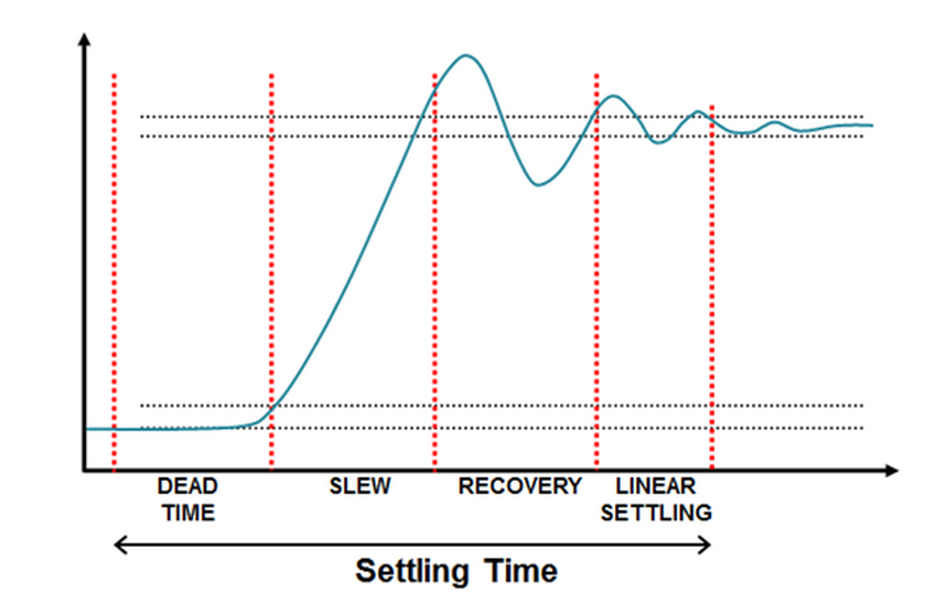
Note: This figure isn’t drawn to scale for any real device; it is exaggerated to show each region
What is settling time?
DAC settling time also bears some striking similarities to op amp settling time. The chief difference, though, is that DAC settling time also includes a figure called dead time. Dead time is the time the DAC spends latching, or updating, its output. This latching action is typically triggered by the falling edge of a digital signal, called LDAC. The LDAC and DAC output interaction is illustrated in the figure below, taken from the DAC8568 datasheet.

If a large input step occurs, the DAC will enter the slew region, which appears in both of the figures above. In the slew region, the DAC’s progress is limited by the slew-rate specification. If the DAC does have to slew, the next phase of setting time will be an overload recovery condition, followed by linear settling time into a specified error band. This error band is typically specified within 1 LSB for the DAC.
The datasheet specification for settling time will be given for a relatively large step-size. The DAC8568, for example, specifies settling time as 5us typical for a change from ¼ full-scale output to ¾ full-scale output.
Keep in mind that slew time can dominate your overall settling time figure, so if your output step-size is smaller than the step-size for the settling time spec in the datasheet, it will take less time for your system to settle. In most high-accuracy applications, settling time is the effective update rate for the DAC.
My next post will be about total unadjusted error, or TUE, a handy way of succinctly describing DAC accuracy. That post will conclude the “DAC Essentials” series on Analog Wire. But Tony and I are not going away. You’ll find us contributing to the TI Precision Designs Hub (“The Hub”), a new blog from Texas Instruments providing precision analog tips, tricks and techniques – from how to read data sheet specs and test conditions to how to optimize the external reference for analog-to-digital (ADC) performance.
An added bonus this week: be sure to check out a new “Engineer It” video about multiplying DACs (MDACs) from my colleague Rahul Prakash.
As always, leave your comments below if you’d like to hear more about anything mentioned in this post, or if there is something you would like to see included in a future post here or on The Hub.
DAC Essentials: What’s with all this glitch-ing?
When designing with a digital-to-analog converter (DAC), you expect the output to move from one value to the next monotonically, but real circuits don’t always behave that way. It’s not uncommon to see overshooting or undershooting, quantified as glitch impulse, across certain code ranges. These impulses can appear in one of two forms, shown below in Figure 1.
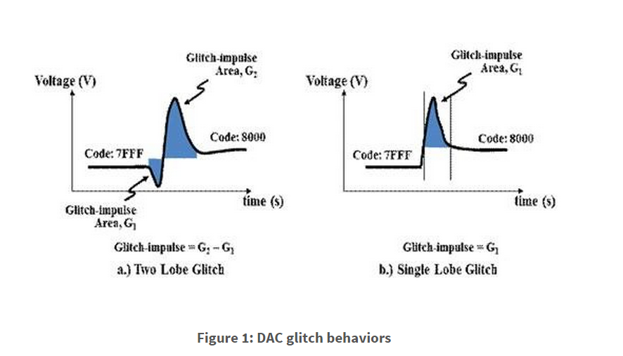
Figure 1a shows a glitch that produces two regions of code transition error, which is common in R-2R precision DACs. Figure 1b shows a single-lobe glitch-impulse, which is more common in string DAC topology. Glitch impulse is quantified as a measure of energy which is commonly specified as nano-Volts-sec (nV-s).
But before we can talk about sources of DAC glitch, we must first define the term “major-carry transition.” A major-carry transition is a single-code transition that causes a most significant bit (MSB) to change because of the lower bits (LSBs) transitioning. Binary code transitions of 0111 to 1000 or 1000 to 0111 are examples of a major-carry transition. Think of it as an inversion of the majority of the switches. This is where glitch-ing is most common.
Two areas of concern are switching synchronization and the switch charge transfer, as multiple switches are simultaneously triggered. For the sake of argument, let’s look at an R2R string DAC that’s designed to rely on switches that are synchronized during code transitions, shown below in Figure 2.
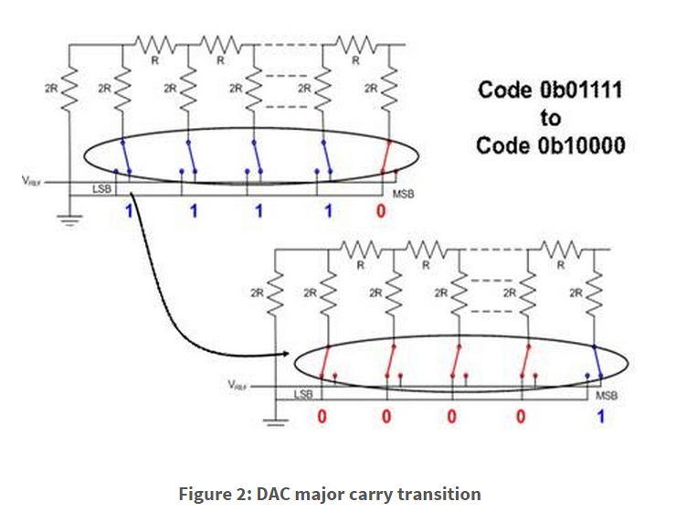
As we all know, there’s no such thing as perfect synchronization, and any variance in the switching will lead to a brief period where all switches are either switched high or low, causing the DAC’s output to error. Recovery occurs and, as a result, a switch charge will create a lobe in the opposite direction, before settling out.
So let’s take a look at the three stages that take place during a major-carry transition and how the DAC output responds, in Figure 3.
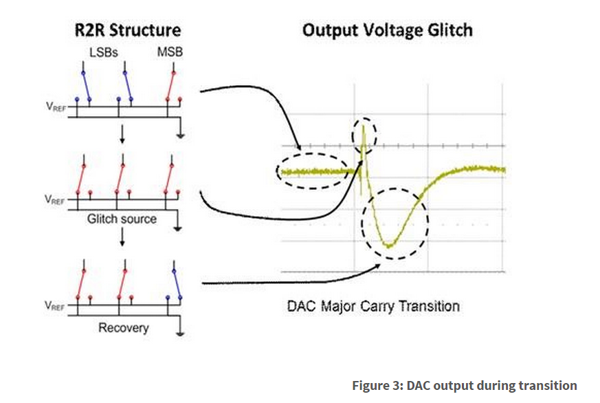
- The initial stage of the DAC, prior to the code transition. In this example we’re looking at the 3 MSBs representing binary code 011.
- The DAC output enters a major-carry transition that causes, for a short period, all of the R-2R switches to be connected to ground.
- The DAC recovers following a small period of switch charge injection, and the output begins to settle out.
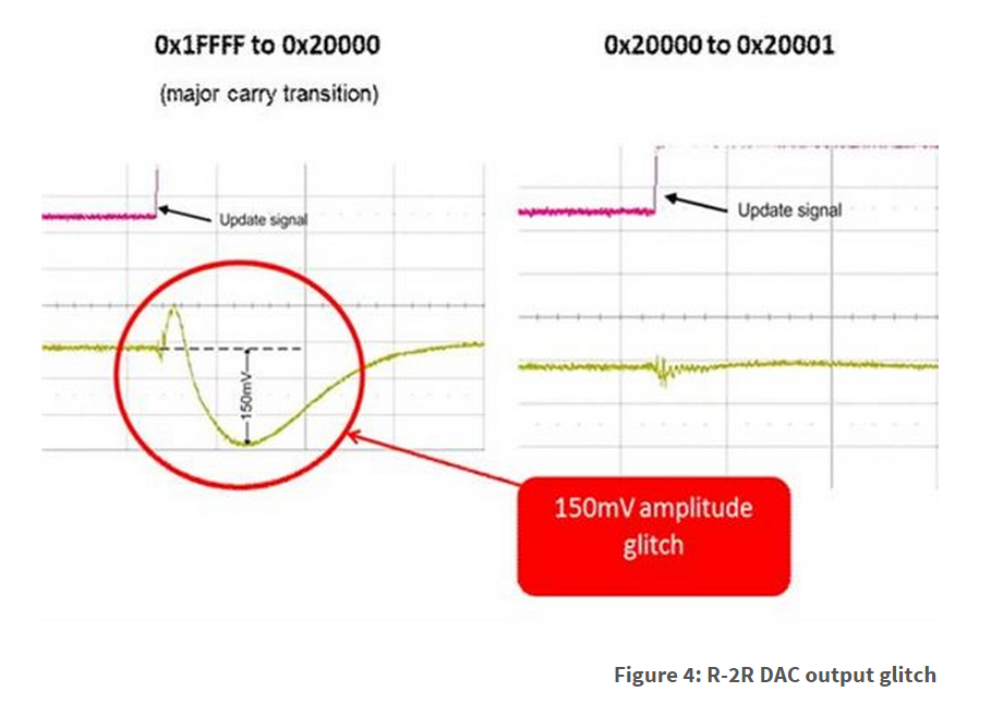
Comparing the output glitch from a major-carry transition versus a non-major-carry transition, illustrated in Figure 4, proves that switching synchronization is the major contributing factor.
X-axis scale is 200ns/div and the Y-axis scale is 50mV/div.
So far, we’ve looked at glitch in an R-2R DAC architecture to explain that switch synchronization is the major contributor. But when you look at the glitch-ing of a string DAC, it is a little different. By design, it taps into different points on a resistor string to produce the output voltage. Without multiple switching, the pulse amplitude is smaller, and often dominated, by digital feedthrough. A comparison of the same major-carry code transition of an R-2R DAC and string DAC topology is shown in Figure 5.

Understanding why glitch-ing occurs can help you decide if your design can live with this short impulse. I’ll talk about some methods to help reduce glitch in the coming weeks.
And if you want to learn more about string and R2R DACs, be sure to check out these previous posts in our DAC Essentials series here on Analog Wire:
- DAC Essentials: String theory on string DACs
- DAC Essentials: The resistor ladder on R-2R DACs
Thanks for reading; I promise my next post will be shorter. :-)
DAC Essentials: Glitch-be-gone
In my last DAC Essentials post, I discussed the source of output glitching in precision digital-to-analog converters (DACs). These output pulses can disrupt system behavior when you’re expecting a linear transition as you step up codes. Let’s take a quick look at a glitch pulse from my previous post as a refresher:
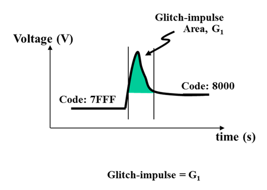
DAC output glitch is an "energy" defined by the width and height of the pulse (shown in green). Manipulating the shape of this glitch may be good enough – depending on the system requirements. Adding a simple RC filter after the DAC output attenuates the amplitude of the glitch but increases settling time. However, the glitch "energy" (area under the curve) remains the same. Below is an example of a DAC crossing a major carry transition showing the output before and after an RC filter.

You should choose the appropriate resistor and capacitor ratio for the RC filter by looking at the glitch period and selecting a cutoff point a decade or so prior. When it comes to picking the component values, you’ll want to keep the resistor value small to avoid a large voltage drop with a resistive load. From the resistor selection, the capacitor value can then be chosen from the desired RC ratio.
Another approach to reduce glitch is using a track and hold amplifier technique. This method is a bit more tedious, as it requires strict switch timing, along with external components leading to higher cost and more board space.
Using an external switch, a few passive components, and amplifier, you can remove the DAC output glitch completely and replace it with a small transient from the new S/H switch. This new short transient can then be attenuated with a first order low pass filter stage. A basic diagram is shown below.

The system design structure is fairly straightforward. The switch is open as the DAC crosses over a major carry transition. This is where the glitch will take place. Once the voltage transition completes, the switch is closed, charging the CH sampling capacitor to the desired value. The capacitor continues to hold the new voltage as the external switch opens while the DAC updates its output again. This allows you to remove the glitch (in theory) without increasing the settling time.
Here are the pros and cons of the two solutions I've discussed:
- If the system can live with increased settling time and needs attenuation on the glitch impulse amplitude, a simple RC filter may do the trick.
- If the system needs the glitch completely removed, a track & hold amplifier solution may work.
Of course, the other option is to steer clear of R-2R DACs and design with a string DAC solution to avoid large glitching altogether. Just know that doing so may force you to tradeoff other DAC specs.
If you’re new to the DAC Essentials series and found this post interesting, be sure to check out our previous posts:
- What’s with all this glitch-ing?
- The resistor ladder
- String theory
- Static specifications & linearity
- The pursuit of perfection
DAC Essentials: Static specifications & linearity
In my last post, “DAC Essentials: The pursuit of perfection,” I explained the concept of the ideal DAC and established the key idioms of its performance. Now we’ll explore how real devices deviate from the ideal DAC transfer function and how to quantify those deviations.
DAC specifications are divided into two basic categories: static and dynamic. Static specifications are behaviors observed at the DAC output at a steady output state, while dynamic specifications refer to behaviors observed during a code-to-code transition. When discussing linearity and the DAC transfer function, you only need to consider static specifications.
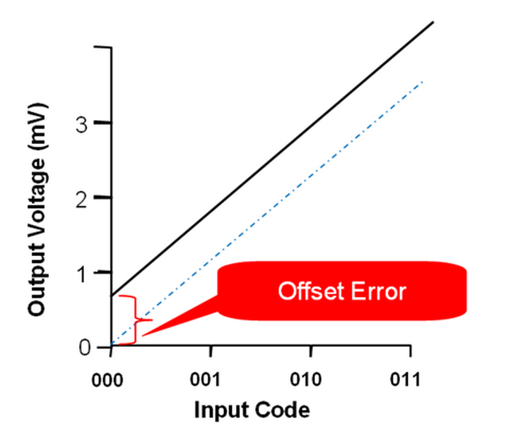
Let’s first start with a spec called offset error. Offset error describes how much the entire DAC transfer function is shifted up or down. The measurement is usually made from a line of best fit taken from a two-point measurement around 10% and 90% full-scale. We do this to avoid operating the output operational amplifier in the non-linear region near its power rails. If you were to consider slope-intercept form for a straight-line equation, y = mx + b, offset error would be the b term, as illustrated below.
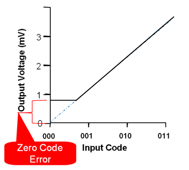
Zero-code error is similar to offset error but describes a different and useful DAC behavior. Zero-code error is measured by loading the DAC with all 0’s and observing the DAC output voltage. In the ideal DAC, we would see 0V at the DAC output when loaded with all 0’s, but due to headroom requirements for the output buffer, we usually see some small offset from 0V.
Another important specification is called gain error. As you may expect, it compares how the real DAC transfer function’s slope relates to the ideal slope. In the ideal case, the slope of the transfer function is equal to exactly 1 LSB, but frequently this figure is slightly off. The measurement for gain error is taken from the same two-point line of best fit used in measuring offset error. If offset error is the b term in y = mx + b, then gain error is the m term.
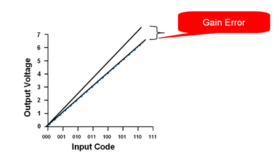
Offset error, zero-code error, and gain error are all provided holistically for a DAC using the measurement techniques mentioned above, which should make sense given what they’re describing. The remaining specifications, INL and DNL, are measured for each and every code in the DAC’s transfer function, but a single number is provided in the electrical characteristics table that expresses the worst case observed across the entire transfer function. The datasheet will also include graphs showing the typical INL or DNL across all codes in the typical characteristics section.
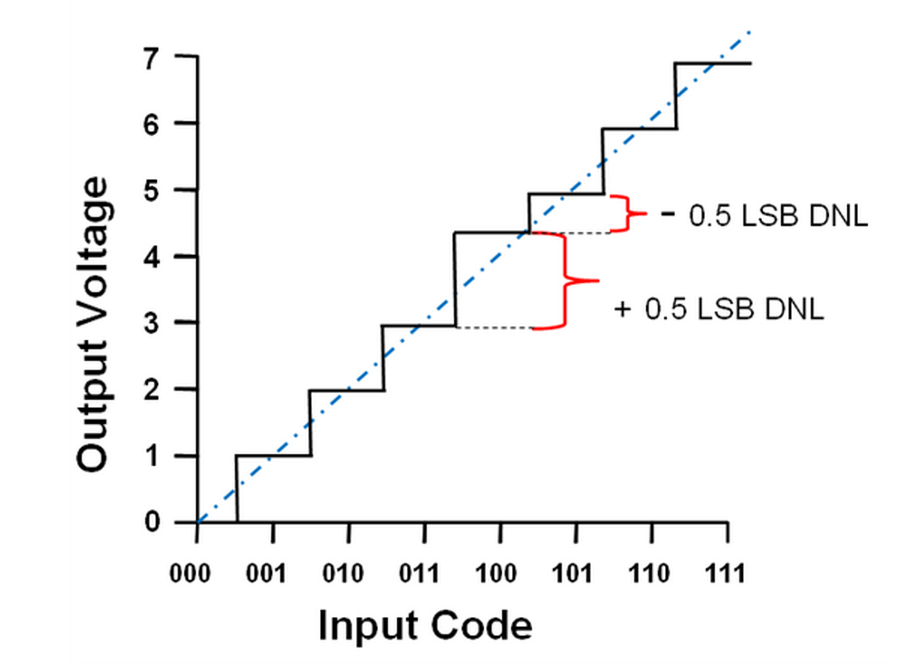
DNL is differential non-linearity. It expresses the difference between measured LSB size and ideal LSB size for any two sequential DAC codes. DNL is often used to infer DAC monotonicity and to determine if the DAC has any missing codes. Since most modern ADCs and DACs are monotonic, DNL is usually not as useful as INL.
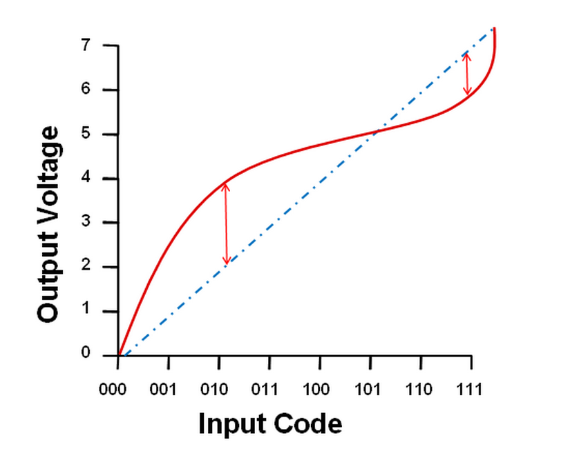
The last static linearity specification is INL – integral non-linearity, which is also referred to as relative accuracy. INL describes the deviation between the ideal output of a DAC and the actual output of a DAC, where offset error and gain error have been calibrated out of the measurement. In a lot of ways, INL is the most valuable specification to consider for an application that requires extremely high precision. Offset, gain, and zero-code errors can be compensated for externally, but there is no way we can reach inside the device package and correct internal mismatches to fix INL.
In our next couple of posts, we’ll take a look at the DAC architectures used to create precision DACs. I hope you’ll check back for them in the coming weeks!
Leave your comments in the section below if you’d like to hear more about anything mentioned in this post or if there is a topic you'd like to see us tackle in the future!
And be sure to check out the full DAC Essentials series!

 浙公网安备 33010602011771号