Fixed DC-DC Regulator Output Uses A Digitally Controlled Potentiometer
Digitally controlled potentiometers (DCPs) have become very popular in a wide variety of applications, including control, parameter adjustment, and signal processing. The digital pots replace mechanical potentiometers and provide advantages such as remote operation and programmability, higher resolution, a much smaller form factor, increased reliability, the ability to store multiple wiper positions, and lower total system cost.
A DCP can be used in many high-end and low-end applications to provide flexibility. For example, a dc-dc regulator can be implemented with a resistor divider in the feedback path to set up VOUT. Some high-end applications need to adjust the voltage to optimize the application’s performance, and that’s where the DCP comes in.
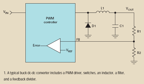
A typical buck dc-dc converter scheme includes a pulse-width modulation (PWM) driver, switches, an inductor, a filter, and a feedback divider (Fig. 1). The feedback voltage (FB) from the resistor divider R1 and R2 is a negative input for the error amplifier of the voltage control loop. In addition to the point-of-load regulation, the feedback divider also sets up the desired output voltage, VOUT. In other words, VOUT is programmable through an external resistor divider based on:

where VREF is a reference voltage and a positive input for the error amplifier.
The minimum output voltage can be set as low as VREF, according to Equation 1. The resistor divider ratio, the input voltage, and the maximum duty cycle determine the maximum output. The reference voltage, VREF, can be obtained from the PWM controller datasheet. Thus, making the feedback divider adjustable makes the dc-dc regulator also adjustable (Fig. 2).
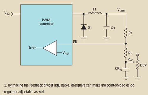
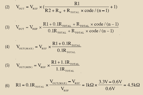
The adjustable output voltage of the dc-dc regulator can be expressed by Equation 2, where R1 and R2 are fixed resistors, RW is the wiper resistance, RTOTAL is the total resistance of the DCP, code is a decimal code of wiper position, and n is the total number of wiper taps.
The advantage of having the DCP in serial with the R2 resistor, rather than in parallel, is easier calculation of dc-dc output. It also prevents the bandwidth limitation that’s specific for the DCP. The DCP terminals have a parasitic capacitance of 10 to 25 pF, shown in Figure 2 as CRW. Connecting any of the DCP terminals to the FB node will cause phase shift and may decrease dc-dc regulator performance, such as transient response and stability.
The right DCP should be chosen to meet the application requirements based on knowing the VOUT adjusting range and desired resolution. For example, we would like to adjust the VOUT output voltage of a dc-dc regulator, built on the ISL85001 PWM controller, from 0.8 to 3.3 V.
The values of the DCP total resistance (RTOTAL) and resistors R1 and R2 can be derived from Equation 2. For simplicity it can be overwritten as Equation 3, where the wiper resistance is counted together with the R2 serial resistor. The suggested value of the R2 resistor should be less or equal to 0.1 × RTOTAL to have a bigger adjusting range (Equation 3, again). The maximum VOUT will be at code = 0 (Equation 4) and the minimum VOUT will be at max code = n – 1 (Equation 5).
According to a sample datasheet (from the ISL85001), the internal VREF = 0.6 V and the recommended value for the R1 resistor is from 1 to 10 kΩ. Since the number of RTOTAL values of the DCPs are limited, let’s select the RTOTAL = 10 kΩ first and then find R1 and R2 (Equation 6):
R1= 4.5k
R2 = 1 kΩ
Thus, the ideal DCP for this example should have an RTOTAL resistance of 10 kΩ and minimum wiper resistance.
Other features should be considered in choosing the appropriate DCP, such as the digital interface, nonvolatile programmability, RTOTAL tolerance, and temperature coefficient (TCr). Most of the available DCPs on the market have ±20% RTOTAL tolerance from part to part. That means each dc-dc regulator requires calibration, and the calibrated value of the wiper position can be stored in nonvolatile memory.
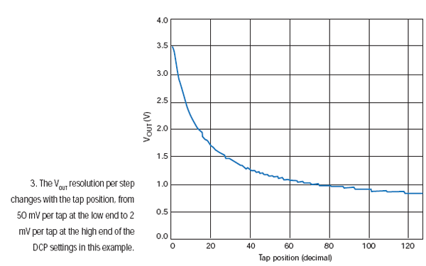
The perfect solution for dc-dc margining uses a 1% precision DCP, like the ISL22317, which eliminates the necessity of individual calibration and provides 0 Ω of wiper resistance and low TCr. Figure 3shows the VOUT curve versus the ISL22317W tap position. Since Equation 2 is a hyperbola, the VOUT resolution per step changes with the tap position, from 50 mV per tap at the low end to 2 mV per tap at the high end of the DCP settings in our example.
The ISL22317 features low TCr and 0 Ω of wiper resistance, complementing Intersil’s compensation scheme while also providing precision resistance settings from –40°C to 125°C.

 浙公网安备 33010602011771号