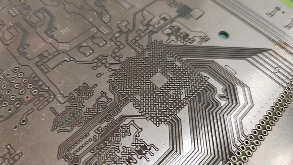
Why does high-speed PCB design need controlled impedance matching?
1. Definition of Impedance Matching
Correctly adjust the output impedance and load impedance of the signal source, adjust the load power, and suppress signal reflection. Its purpose is to ensure that the signal or energy can be efficiently transferred from the signal source to the load.
Second, the reason for impedance matching
Resistor matching may not be used in low-speed PCBs, but complete, reliable, accurate, interference-free, and noise-free transmission signals must be provided when designing high-speed PCBs. Therefore, it is necessary to ensure that the characteristics of the PCB circuit are reflected in the transmission process, the signal is complete, the transmission loss is low, and it plays the role of matching impedance. If critical signals are not matched to resistors, it can cause signal reflections, bounces, loss, etc. UART-модуль
3. Factors Affecting Impedance
1. By changing the thickness of the medium, the impedance will also change. The thickness of the medium is proportional to the impedance; different prepregs have different glue content and thickness. The compression thickness depends on the press layout and platen program; for any material used, it is necessary to obtain the thickness of the insulating layer that can be produced for easy calculation, and engineering design, platen control, and material tolerance are the keys to adjusting the thickness of the medium.
2. T-line width, increasing the line width can reduce the impedance, and reducing the line width can increase the impedance. In order to better meet the requirements of the impedance test line, a tolerance of ±10% is required to control the line width. The breakdown of the impedance test line affects the entire test waveform, and its single-point resistance is high, resulting in misalignment of the entire waveform. Impedance lines are not allowed, and the breakdown does not exceed 10%. Linewidth is mainly controlled by etch. In order to ensure the line width, the line width requirements should be met according to the etching, lithography error, graphic shear error and technical film compensation technology.
3. The thicker the copper, the thinner the wire, the greater the impedance; the thicker the wire, the smaller the impedance. The thickness of the wires can be controlled by sample plating or by selecting a substrate with an appropriate thickness. Copper thickness should be controlled evenly. Add bypass blocks on thin wire and insulated wire boards to balance the current, avoid uneven copper thickness on the lines, affect impedance, and make uneven copper distribution on CS and SS surfaces. To achieve an even copper thickness on both sides, the board must be pulled across.
4. Er-dielectric constant. Different board materials have different dielectric constants. Common board materials include paper substrates, epoxy glass fiber cloth substrates (FR4 is more commonly used), and composite substrates. FR4 is commonly used. The Er characteristic of the material changes with the loading frequency. It is considered to be about 4.2 when the use frequency is below 1GHZ, and it will decrease under the use frequency of 1.5-2.0GHZ. Therefore, it is necessary to pay attention to the use frequency of the product in practical applications.
5. Resistance welding thickness and pressure resistance welding reduce the outer resistance. Under normal circumstances, one resistance welding print can reduce single-ended 2 ohms and differential 8 ohms. Printing twice reduces the value twice as much as printing once. If printed more than three times, the impedance value will not change.
4. What types of impedance lines are there?
The first one is a single-line microstrip line, and the second is a differential stripline. Of course, the microstrip line can also have differential, and the stripline can also have single-ended.
In multilayer boards, unidirectional and differential wires refer to adjacent layers. It is important to note that the RF line processing is referred to as the middle layer, providing the optimum RF antenna width for best performance. The so-called parallel resistance refers to a unidirectional or multi-directional line that requires resistance matching, and usually includes copper plates on both sides of the signal line to achieve the goal of resistance matching. As shown in the picture:
5. What are the lines that usually need to control impedance? How much Ω is needed? GPS-модуль
Different signals have different impedance values, such as 90Ω, 100Ω, 120Ω, and so on. Not all lines have impedance matching requirements. Universal USB2.0 requires 90Ω impedance, HDMI, USB3.0, MIPI, 100M ports, Gigabit ports and other controls are usually 100Ω impedance, RS422 is 120Ω. A unipolar line is usually a counter resistance of 50Ω, ideally 50Ω. However, in fact the full source resistance is not 50Ω, nor is the load connection resistance. At this point, several resistive contacts are required, and the proper circuit consists of inductors and capacitors. At the same time, we need to use capacitors and inductors to tune the resistor tuning circuit to achieve the best RF characteristics.
 Correctly adjust the output impedance and load impedance of the signal source, adjust the load power, and suppress signal reflection. Its purpose is to ensure that the signal or energy can be efficiently transferred from the signal source to the load.

 浙公网安备 33010602011771号