
STM32:SPI
1 SPI协议
SPI全称serial peripheral interface,串行外设接口;为串行通讯接口协议;
spi接口通过NSS、SCK、MISO、MOSI四线同其他设备相连,每个slave都需要一条独立的NSS,SCK总是由master提供;
spi接口作为常用的板间通信协议,常用在ADC,LCD,EEPROM和FLASH存储器上;
spi接口时序要求低,传输速率快,没有应答位;通讯速率最高为APB的二分频;
1.1 工作模式
mode[1:0] = mode[ CPOL : CPHA ],有四种模式;
CPOL:clock polarity 时钟极性,决定SCK的起始电平是0还是1,CPOL=0表示时钟的起始电平为低;
CPHA:clock phase 时钟相位,决定数据采样点是在SCK的第1个跳变沿还是第二个跳变沿,CPHA=0表示取样点为第一个跳变沿;
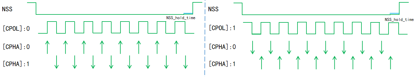
目前遇到的SPI协议清一色是模式0;w25qxx只支持模式0和模式3的全双工从模式spi协议,数据采样点都是在上升沿;
上升沿通常由D触发器生成,信号较为稳定;下降沿的触发器触发时会有一些组合逻辑的延时,不如上升沿稳定;
有效数据应该在数据采样点之前放入寄存器中;意思是如果数据是在上升沿采样,那么数据在下降沿触发变化;
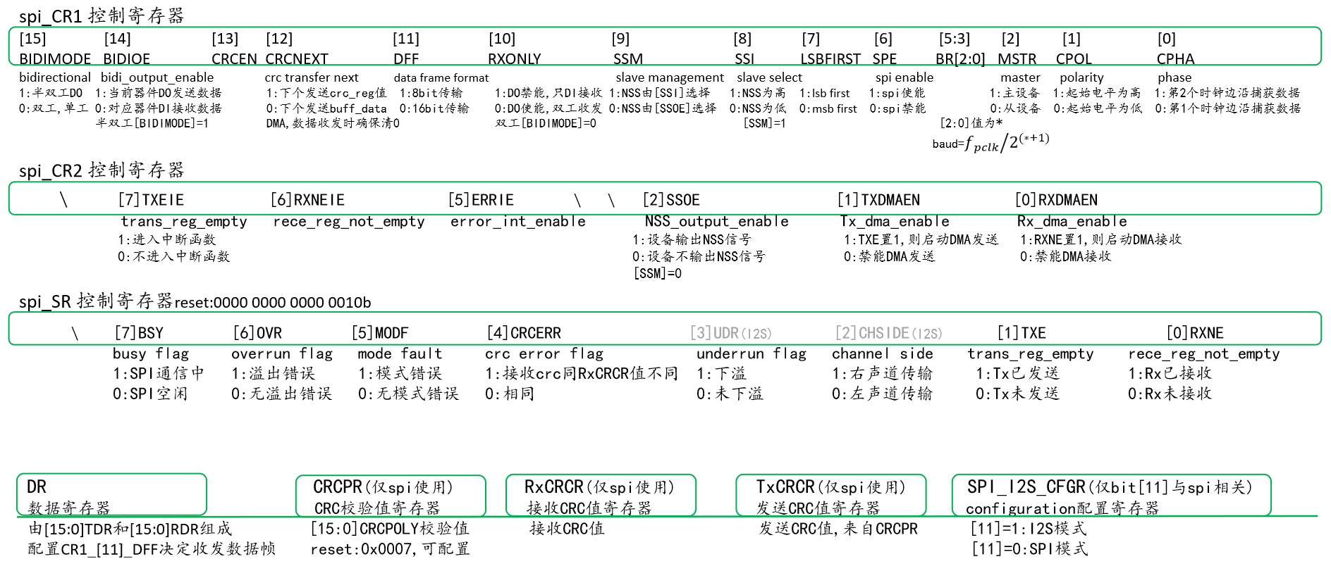
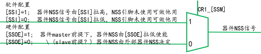
2 SPI寄存器
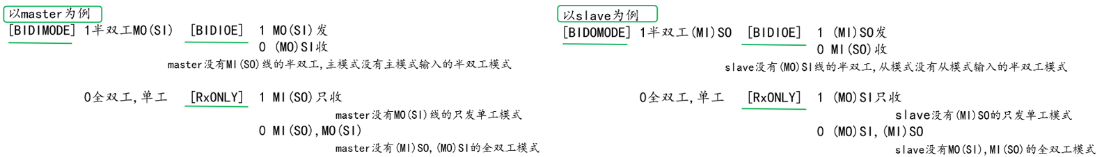
为什么单工的1-line是bidirectional,而双工的2-line是unidirectional我想了一个小时也没想明白,我决定不想了;
可能是因为bidirectional不应该理解成单工,而应该理解成半双工;而双工的2-line_unidirectional 是说没有分时复用都是单向的;
3 标准库函数
3.1 结构体封装
typedef struct SPI_TypeDef
/***stm32f10x.h  地址映射***/

typedef struct
{
  __IO uint16_t CR1;
  uint16_t  RESERVED0;
  __IO uint16_t CR2;
  uint16_t  RESERVED1;
  __IO uint16_t SR;
  uint16_t  RESERVED2;
  __IO uint16_t DR;
  uint16_t  RESERVED3;
  __IO uint16_t CRCPR;
  uint16_t  RESERVED4;
  __IO uint16_t RXCRCR;
  uint16_t  RESERVED5;
  __IO uint16_t TXCRCR;
  uint16_t  RESERVED6;
  __IO uint16_t I2SCFGR;
  uint16_t  RESERVED7;
  __IO uint16_t I2SPR;
  uint16_t  RESERVED8;
} SPI_TypeDef;

#define SPI2                  ((SPI_TypeDef *) SPI2_BASE)
#define SPI2_BASE             (APB1PERIPH_BASE + 0x3800)
#define APB1PERIPH_BASE        PERIPH_BASE
#define PERIPH_BASE           ((uint32_t)0x40000000)
typedef struct SPI_InitTypeDef
/***stm32f10x_spi.h***/
typedef struct
{
  uint16_t SPI_Direction;
  uint16_t SPI_Mode;
  uint16_t SPI_DataSize;
  uint16_t SPI_CPOL;
  uint16_t SPI_CPHA;
  uint16_t SPI_NSS;
  uint16_t SPI_BaudRatePrescaler;
  uint16_t SPI_FirstBit;
  uint16_t SPI_CRCPolynomial;
}SPI_InitTypeDef;

#define SPI_Direction_2Lines_FullDuplex ((uint16_t)0x0000)
#define SPI_Direction_2Lines_RxOnly     ((uint16_t)0x0400)
#define SPI_Direction_1Line_Rx          ((uint16_t)0x8000)
#define SPI_Direction_1Line_Tx          ((uint16_t)0xC000)

#define SPI_Mode_Master                 ((uint16_t)0x0104)
#define SPI_Mode_Slave                  ((uint16_t)0x0000)

#define SPI_DataSize_16b                ((uint16_t)0x0800)
#define SPI_DataSize_8b                 ((uint16_t)0x0000)

#define SPI_CPOL_Low                    ((uint16_t)0x0000)
#define SPI_CPOL_High                   ((uint16_t)0x0002)

#define SPI_CPHA_1Edge                  ((uint16_t)0x0000)
#define SPI_CPHA_2Edge                  ((uint16_t)0x0001)

#define SPI_NSS_Soft                    ((uint16_t)0x0200)
#define SPI_NSS_Hard                    ((uint16_t)0x0000)

#define SPI_BaudRatePrescaler_2         ((uint16_t)0x0000)
#define SPI_BaudRatePrescaler_4         ((uint16_t)0x0008)
#define SPI_BaudRatePrescaler_8         ((uint16_t)0x0010)
#define SPI_BaudRatePrescaler_16        ((uint16_t)0x0018)
#define SPI_BaudRatePrescaler_32        ((uint16_t)0x0020)
#define SPI_BaudRatePrescaler_64        ((uint16_t)0x0028)
#define SPI_BaudRatePrescaler_128       ((uint16_t)0x0030)
#define SPI_BaudRatePrescaler_256       ((uint16_t)0x0038)

#define SPI_FirstBit_MSB                ((uint16_t)0x0000)
#define SPI_FirstBit_LSB                ((uint16_t)0x0080)

#define IS_SPI_CRC_POLYNOMIAL(POLYNOMIAL) ((POLYNOMIAL) >= 0x1)
3.2 标准库函数
SPI_I2S_DeInit(SPI_TypeDef* SPIx)
void SPI_I2S_DeInit(SPI_TypeDef* SPIx)
{
  /* Check the parameters */
  assert_param(IS_SPI_ALL_PERIPH(SPIx));

  if (SPIx == SPI1)
  {
    /* Enable SPI1 reset state */
    RCC_APB2PeriphResetCmd(RCC_APB2Periph_SPI1, ENABLE);
    /* Release SPI1 from reset state */
    RCC_APB2PeriphResetCmd(RCC_APB2Periph_SPI1, DISABLE);
  }
  else if (SPIx == SPI2)
  {
    /* Enable SPI2 reset state */
    RCC_APB1PeriphResetCmd(RCC_APB1Periph_SPI2, ENABLE);
    /* Release SPI2 from reset state */
    RCC_APB1PeriphResetCmd(RCC_APB1Periph_SPI2, DISABLE);
  }
  else
  {
    if (SPIx == SPI3)
    {
      /* Enable SPI3 reset state */
      RCC_APB1PeriphResetCmd(RCC_APB1Periph_SPI3, ENABLE);
      /* Release SPI3 from reset state */
      RCC_APB1PeriphResetCmd(RCC_APB1Periph_SPI3, DISABLE);
    }
  }
}
SPI_Init(SPI_TypeDef* SPIx, SPI_InitTypeDef* SPI_InitStruct)
/***stm32f10x_spi.c***/

#define CR1_CLEAR_Mask            ((uint16_t)0xE9F3)  /*1110 1001 1111 0011b,清0[12],[10],[9],[3],[2]*/
#define SPI_Mode_Select      ((uint16_t)0xF7FF)
#define I2S_Mode_Select      ((uint16_t)0x0800)

void SPI_Init(SPI_TypeDef* SPIx, SPI_InitTypeDef* SPI_InitStruct)
{
  uint16_t tmpreg = 0;

  /* check the parameters */
  assert_param(IS_SPI_ALL_PERIPH(SPIx));

  /* Check the SPI parameters */
  assert_param(IS_SPI_DIRECTION_MODE(SPI_InitStruct->SPI_Direction));
  assert_param(IS_SPI_MODE(SPI_InitStruct->SPI_Mode));
  assert_param(IS_SPI_DATASIZE(SPI_InitStruct->SPI_DataSize));
  assert_param(IS_SPI_CPOL(SPI_InitStruct->SPI_CPOL));
  assert_param(IS_SPI_CPHA(SPI_InitStruct->SPI_CPHA));
  assert_param(IS_SPI_NSS(SPI_InitStruct->SPI_NSS));
  assert_param(IS_SPI_BAUDRATE_PRESCALER(SPI_InitStruct->SPI_BaudRatePrescaler));
  assert_param(IS_SPI_FIRST_BIT(SPI_InitStruct->SPI_FirstBit));
  assert_param(IS_SPI_CRC_POLYNOMIAL(SPI_InitStruct->SPI_CRCPolynomial));

/*---------------------------- SPIx CR1 Configuration ------------------------*/
  tmpreg = SPIx->CR1;
  tmpreg &= CR1_CLEAR_Mask;
  tmpreg |= (uint16_t)((uint32_t)SPI_InitStruct->SPI_Direction | SPI_InitStruct->SPI_Mode |
                  SPI_InitStruct->SPI_DataSize | SPI_InitStruct->SPI_CPOL |
                  SPI_InitStruct->SPI_CPHA | SPI_InitStruct->SPI_NSS |
                  SPI_InitStruct->SPI_BaudRatePrescaler | SPI_InitStruct->SPI_FirstBit);
  SPIx->CR1 = tmpreg;

  /* Activate the SPI mode (Reset I2SMOD bit in I2SCFGR register) */
  SPIx->I2SCFGR &= SPI_Mode_Select;

/*---------------------------- SPIx CRCPOLY Configuration --------------------*/
  /* Write to SPIx CRCPOLY */
  SPIx->CRCPR = SPI_InitStruct->SPI_CRCPolynomial;
}
SPI_StructInit(SPI_InitTypeDef* SPI_InitStruct)
 /***spi初始化例程***/
void SPI_StructInit(SPI_InitTypeDef* SPI_InitStruct)
{
/*--------------- Reset SPI init structure parameters values -----------------*/
  /* Initialize the SPI_Direction member */
  SPI_InitStruct->SPI_Direction = SPI_Direction_2Lines_FullDuplex;
  /* initialize the SPI_Mode member */
  SPI_InitStruct->SPI_Mode = SPI_Mode_Slave;
  /* initialize the SPI_DataSize member */
  SPI_InitStruct->SPI_DataSize = SPI_DataSize_8b;
  /* Initialize the SPI_CPOL member */
  SPI_InitStruct->SPI_CPOL = SPI_CPOL_Low;
  /* Initialize the SPI_CPHA member */
  SPI_InitStruct->SPI_CPHA = SPI_CPHA_1Edge;
  /* Initialize the SPI_NSS member */
  SPI_InitStruct->SPI_NSS = SPI_NSS_Hard;
  /* Initialize the SPI_BaudRatePrescaler member */
  SPI_InitStruct->SPI_BaudRatePrescaler = SPI_BaudRatePrescaler_2;
  /* Initialize the SPI_FirstBit member */
  SPI_InitStruct->SPI_FirstBit = SPI_FirstBit_MSB;
  /* Initialize the SPI_CRCPolynomial member */
  SPI_InitStruct->SPI_CRCPolynomial = 7;
}
SPI_Cmd(SPI_TypeDef* SPIx, FunctionalState NewState)
 /* SPI SPE mask */
#define CR1_SPE_Set          ((uint16_t)0x0040)
#define CR1_SPE_Reset        ((uint16_t)0xFFBF)

void SPI_Cmd(SPI_TypeDef* SPIx, FunctionalState NewState)
{
  /* Check the parameters */
  assert_param(IS_SPI_ALL_PERIPH(SPIx));
  assert_param(IS_FUNCTIONAL_STATE(NewState));
  if (NewState != DISABLE)
  {
    /* Enable the selected SPI peripheral */
    SPIx->CR1 |= CR1_SPE_Set;
  }
  else
  {
    /* Disable the selected SPI peripheral */
    SPIx->CR1 &= CR1_SPE_Reset;
  }
}
SPI_I2S_ITConfig(SPI_TypeDef* SPIx, uint8_t SPI_I2S_IT, FunctionalState NewState)
/***stm32f10x_spi.h***/
#define SPI_I2S_IT_TXE                  ((uint8_t)0x71)
#define SPI_I2S_IT_RXNE                 ((uint8_t)0x60)
#define SPI_I2S_IT_ERR                  ((uint8_t)0x50)
#define IS_SPI_I2S_CONFIG_IT(IT) (((IT) == SPI_I2S_IT_TXE) || \
                                 ((IT) == SPI_I2S_IT_RXNE) || \
                                 ((IT) == SPI_I2S_IT_ERR))

/***stm32f10x_spi.c***/
void SPI_I2S_ITConfig(SPI_TypeDef* SPIx, uint8_t SPI_I2S_IT, FunctionalState NewState)
{
  uint16_t itpos = 0, itmask = 0 ;
  /* Check the parameters */
  assert_param(IS_SPI_ALL_PERIPH(SPIx));
  assert_param(IS_FUNCTIONAL_STATE(NewState));
  assert_param(IS_SPI_I2S_CONFIG_IT(SPI_I2S_IT));

  /* Get the SPI/I2S IT index */
  itpos = SPI_I2S_IT >> 4;

  /* Set the IT mask */
  itmask = (uint16_t)1 << (uint16_t)itpos;

  if (NewState != DISABLE)
  {
    /* Enable the selected SPI/I2S interrupt */
    SPIx->CR2 |= itmask;
  }
  else
  {
    /* Disable the selected SPI/I2S interrupt */
    SPIx->CR2 &= (uint16_t)~itmask;
  }
}
SPI_I2S_DMACmd(SPI_TypeDef* SPIx, uint16_t SPI_I2S_DMAReq, FunctionalState NewState)
 /***stm32f10x_spi.h***/
#define SPI_I2S_DMAReq_Tx               ((uint16_t)0x0002)
#define SPI_I2S_DMAReq_Rx               ((uint16_t)0x0001)
#define IS_SPI_I2S_DMAREQ(DMAREQ) ((((DMAREQ) & (uint16_t)0xFFFC) == 0x00) && ((DMAREQ) != 0x00))

/***stm32f10x_spi.c***/
void SPI_I2S_DMACmd(SPI_TypeDef* SPIx, uint16_t SPI_I2S_DMAReq, FunctionalState NewState)
{
  /* Check the parameters */
  assert_param(IS_SPI_ALL_PERIPH(SPIx));
  assert_param(IS_FUNCTIONAL_STATE(NewState));
  assert_param(IS_SPI_I2S_DMAREQ(SPI_I2S_DMAReq));
  if (NewState != DISABLE)
  {
    /* Enable the selected SPI/I2S DMA requests */
    SPIx->CR2 |= SPI_I2S_DMAReq;
  }
  else
  {
    /* Disable the selected SPI/I2S DMA requests */
    SPIx->CR2 &= (uint16_t)~SPI_I2S_DMAReq;
  }
}
SPI_I2S_SendData(SPI_TypeDef* SPIx, uint16_t Data)
 void SPI_I2S_SendData(SPI_TypeDef* SPIx, uint16_t Data)
{
  /* Check the parameters */
  assert_param(IS_SPI_ALL_PERIPH(SPIx));

  /* Write in the DR register the data to be sent */
  SPIx->DR = Data;
}
SPI_I2S_ReceiveData(SPI_TypeDef* SPIx)
 uint16_t SPI_I2S_ReceiveData(SPI_TypeDef* SPIx)
{
  /* Check the parameters */
  assert_param(IS_SPI_ALL_PERIPH(SPIx));

  /* Return the data in the DR register */
  return SPIx->DR;
}
SPI_NSSInternalSoftwareConfig(SPI_TypeDef* SPIx, uint16_t SPI_NSSInternalSoft)
 /***stm32f10x_spi.h***/
#define SPI_NSSInternalSoft_Set         ((uint16_t)0x0100)
#define SPI_NSSInternalSoft_Reset       ((uint16_t)0xFEFF)
#define IS_SPI_NSS_INTERNAL(INTERNAL) (((INTERNAL) == SPI_NSSInternalSoft_Set) || \
                                       ((INTERNAL) == SPI_NSSInternalSoft_Reset))
/***stm32f10x_spi.c***/
void SPI_NSSInternalSoftwareConfig(SPI_TypeDef* SPIx, uint16_t SPI_NSSInternalSoft)
{
  /* Check the parameters */
  assert_param(IS_SPI_ALL_PERIPH(SPIx));
  assert_param(IS_SPI_NSS_INTERNAL(SPI_NSSInternalSoft));
  if (SPI_NSSInternalSoft != SPI_NSSInternalSoft_Reset)
  {
    /* Set NSS pin internally by software */
    SPIx->CR1 |= SPI_NSSInternalSoft_Set;
  }
  else
  {
    /* Reset NSS pin internally by software */
    SPIx->CR1 &= SPI_NSSInternalSoft_Reset;
  }
}
SPI_SSOutputCmd(SPI_TypeDef* SPIx, FunctionalState NewState)
 /* SPI SSOE mask */
#define CR2_SSOE_Set         ((uint16_t)0x0004)
#define CR2_SSOE_Reset       ((uint16_t)0xFFFB)

void SPI_SSOutputCmd(SPI_TypeDef* SPIx, FunctionalState NewState)
{
  /* Check the parameters */
  assert_param(IS_SPI_ALL_PERIPH(SPIx));
  assert_param(IS_FUNCTIONAL_STATE(NewState));
  if (NewState != DISABLE)
  {
    /* Enable the selected SPI SS output */
    SPIx->CR2 |= CR2_SSOE_Set;
  }
  else
  {
    /* Disable the selected SPI SS output */
    SPIx->CR2 &= CR2_SSOE_Reset;
  }
}
SPI_DataSizeConfig(SPI_TypeDef* SPIx, uint16_t SPI_DataSize)
 /***stm32f10x_spi.h***/
#define SPI_DataSize_16b                ((uint16_t)0x0800)
#define SPI_DataSize_8b                 ((uint16_t)0x0000)
#define IS_SPI_DATASIZE(DATASIZE) (((DATASIZE) == SPI_DataSize_16b) || \
                                   ((DATASIZE) == SPI_DataSize_8b))

/***stm32f10x_spi.c***/
void SPI_DataSizeConfig(SPI_TypeDef* SPIx, uint16_t SPI_DataSize)
{
  /* Check the parameters */
  assert_param(IS_SPI_ALL_PERIPH(SPIx));
  assert_param(IS_SPI_DATASIZE(SPI_DataSize));
  /* Clear DFF bit */
  SPIx->CR1 &= (uint16_t)~SPI_DataSize_16b;
  /* Set new DFF bit value */
  SPIx->CR1 |= SPI_DataSize;
}
SPI_TransmitCRC(SPI_TypeDef* SPIx)
 /* SPI CRCNext mask */
#define CR1_CRCNext_Set      ((uint16_t)0x1000)

void SPI_TransmitCRC(SPI_TypeDef* SPIx)
{
  /* Check the parameters */
  assert_param(IS_SPI_ALL_PERIPH(SPIx));

  /* Enable the selected SPI CRC transmission */
  SPIx->CR1 |= CR1_CRCNext_Set;
}
SPI_CalculateCRC(SPI_TypeDef* SPIx, FunctionalState NewState)
 /* SPI CRCEN mask   是否使能[CRCEN]位;*/
#define CR1_CRCEN_Set        ((uint16_t)0x2000)
#define CR1_CRCEN_Reset      ((uint16_t)0xDFFF)

void SPI_CalculateCRC(SPI_TypeDef* SPIx, FunctionalState NewState)
{
  /* Check the parameters */
  assert_param(IS_SPI_ALL_PERIPH(SPIx));
  assert_param(IS_FUNCTIONAL_STATE(NewState));
  if (NewState != DISABLE)
  {
    /* Enable the selected SPI CRC calculation */
    SPIx->CR1 |= CR1_CRCEN_Set;
  }
  else
  {
    /* Disable the selected SPI CRC calculation */
    SPIx->CR1 &= CR1_CRCEN_Reset;
  }
}
SPI_GetCRC(SPI_TypeDef* SPIx, uint8_t SPI_CRC)
 /***stm32f10x_spi.h***/
#define SPI_CRC_Tx                      ((uint8_t)0x00)
#define SPI_CRC_Rx                      ((uint8_t)0x01)
#define IS_SPI_CRC(CRC) (((CRC) == SPI_CRC_Tx) || ((CRC) == SPI_CRC_Rx))

/***stm32f10x_spi.c***/
uint16_t SPI_GetCRC(SPI_TypeDef* SPIx, uint8_t SPI_CRC)
{
  uint16_t crcreg = 0;
  /* Check the parameters */
  assert_param(IS_SPI_ALL_PERIPH(SPIx));
  assert_param(IS_SPI_CRC(SPI_CRC));
  if (SPI_CRC != SPI_CRC_Rx)
  {
    /* Get the Tx CRC register */
    crcreg = SPIx->TXCRCR;
  }
  else
  {
    /* Get the Rx CRC register */
    crcreg = SPIx->RXCRCR;
  }
  /* Return the selected CRC register */
  return crcreg;
}
SPI_GetCRCPolynomial(SPI_TypeDef* SPIx)
 uint16_t SPI_GetCRCPolynomial(SPI_TypeDef* SPIx)
{
  /* Check the parameters */
  assert_param(IS_SPI_ALL_PERIPH(SPIx));

  /* Return the CRC polynomial register */
  return SPIx->CRCPR;
}
SPI_I2S_ClearFlag(SPI_TypeDef* SPIx, uint16_t SPI_I2S_FLAG)
 /***stm32f10x_spi.h***/
#define SPI_FLAG_CRCERR                 ((uint16_t)0x0010)
#define IS_SPI_I2S_CLEAR_FLAG(FLAG) (((FLAG) == SPI_FLAG_CRCERR))

/***stm32f10x_spi.c  这个函数虽然叫clear flag,但是它只清除[CRCERR];小离谱***/
void SPI_I2S_ClearFlag(SPI_TypeDef* SPIx, uint16_t SPI_I2S_FLAG)
{
  /* Check the parameters */
  assert_param(IS_SPI_ALL_PERIPH(SPIx));
  assert_param(IS_SPI_I2S_CLEAR_FLAG(SPI_I2S_FLAG));

    /* Clear the selected SPI CRC Error (CRCERR) flag */
    SPIx->SR = (uint16_t)~SPI_I2S_FLAG;
}
SPI_I2S_ClearITPendingBit(SPI_TypeDef* SPIx, uint8_t SPI_I2S_IT)
 /***stm32f10x_spi.h***/
#define SPI_IT_CRCERR                   ((uint8_t)0x54)
#define IS_SPI_I2S_CLEAR_IT(IT) (((IT) == SPI_IT_CRCERR))

/***stm32f10x_spi.c***/
void SPI_I2S_ClearITPendingBit(SPI_TypeDef* SPIx, uint8_t SPI_I2S_IT)
{
  uint16_t itpos = 0;
  /* Check the parameters */
  assert_param(IS_SPI_ALL_PERIPH(SPIx));
  assert_param(IS_SPI_I2S_CLEAR_IT(SPI_I2S_IT));

  /* Get the SPI IT index */
  itpos = 0x01 << (SPI_I2S_IT & 0x0F);

  /* Clear the selected SPI CRC Error (CRCERR) interrupt pending bit */
  SPIx->SR = (uint16_t)~itpos;
}
SPI_BiDirectionalLineConfig(SPI_TypeDef* SPIx, uint16_t SPI_Direction)
 /***stm32f10x_spi.h***/
#define SPI_Direction_Rx                ((uint16_t)0xBFFF)
#define SPI_Direction_Tx                ((uint16_t)0x4000)
#define IS_SPI_DIRECTION(DIRECTION) (((DIRECTION) == SPI_Direction_Rx) || \
                                     ((DIRECTION) == SPI_Direction_Tx))

/***stm32f10x_spi.c***/
void SPI_BiDirectionalLineConfig(SPI_TypeDef* SPIx, uint16_t SPI_Direction)
{
  /* Check the parameters */
  assert_param(IS_SPI_ALL_PERIPH(SPIx));
  assert_param(IS_SPI_DIRECTION(SPI_Direction));
  if (SPI_Direction == SPI_Direction_Tx)
  {
    /* Set the Tx only mode */
    SPIx->CR1 |= SPI_Direction_Tx;
  }
  else
  {
    /* Set the Rx only mode */
    SPIx->CR1 &= SPI_Direction_Rx;
  }
}
SPI_I2S_GetFlagStatus(SPI_TypeDef* SPIx, uint16_t SPI_I2S_FLAG)
  /***stm32f10x_spi.h***/
#define SPI_I2S_FLAG_RXNE               ((uint16_t)0x0001)
#define SPI_I2S_FLAG_TXE                ((uint16_t)0x0002)
#define I2S_FLAG_CHSIDE                 ((uint16_t)0x0004)
#define I2S_FLAG_UDR                    ((uint16_t)0x0008)
#define SPI_FLAG_CRCERR                 ((uint16_t)0x0010)
#define SPI_FLAG_MODF                   ((uint16_t)0x0020)
#define SPI_I2S_FLAG_OVR                ((uint16_t)0x0040)
#define SPI_I2S_FLAG_BSY                ((uint16_t)0x0080)
#define IS_SPI_I2S_CLEAR_FLAG(FLAG) (((FLAG) == SPI_FLAG_CRCERR))
#define IS_SPI_I2S_GET_FLAG(FLAG) (((FLAG) == SPI_I2S_FLAG_BSY) || ((FLAG) == SPI_I2S_FLAG_OVR) || \
                                   ((FLAG) == SPI_FLAG_MODF) || ((FLAG) == SPI_FLAG_CRCERR) || \
                                   ((FLAG) == I2S_FLAG_UDR) || ((FLAG) == I2S_FLAG_CHSIDE) || \
                                   ((FLAG) == SPI_I2S_FLAG_TXE) || ((FLAG) == SPI_I2S_FLAG_RXNE))

 /***stm32f10x_spi.c***/
FlagStatus SPI_I2S_GetFlagStatus(SPI_TypeDef* SPIx, uint16_t SPI_I2S_FLAG)
{
  FlagStatus bitstatus = RESET;
  /* Check the parameters */
  assert_param(IS_SPI_ALL_PERIPH(SPIx));
  assert_param(IS_SPI_I2S_GET_FLAG(SPI_I2S_FLAG));
  /* Check the status of the specified SPI/I2S flag */
  if ((SPIx->SR & SPI_I2S_FLAG) != (uint16_t)RESET)
  {
    /* SPI_I2S_FLAG is set */
    bitstatus = SET;
  }
  else
  {
    /* SPI_I2S_FLAG is reset */
    bitstatus = RESET;
  }
  /* Return the SPI_I2S_FLAG status */
  return  bitstatus;
}
SPI_I2S_GetITStatus(SPI_TypeDef* SPIx, uint8_t SPI_I2S_IT)
 /***stm32f10x_spi.h***/
#define SPI_I2S_IT_TXE                  ((uint8_t)0x71)
#define SPI_I2S_IT_RXNE                 ((uint8_t)0x60)

#define SPI_I2S_IT_OVR                  ((uint8_t)0x56)
#define SPI_IT_MODF                     ((uint8_t)0x55)
#define SPI_IT_CRCERR                   ((uint8_t)0x54)
#define I2S_IT_UDR                      ((uint8_t)0x53)

#define IS_SPI_I2S_GET_IT(IT) (((IT) == SPI_I2S_IT_RXNE) || ((IT) == SPI_I2S_IT_TXE) || \
                               ((IT) == I2S_IT_UDR) || ((IT) == SPI_IT_CRCERR) || \
                               ((IT) == SPI_IT_MODF) || ((IT) == SPI_I2S_IT_OVR))

/***stm32f10x_spi.c***/
ITStatus SPI_I2S_GetITStatus(SPI_TypeDef* SPIx, uint8_t SPI_I2S_IT)
{
  ITStatus bitstatus = RESET;
  uint16_t itpos = 0, itmask = 0, enablestatus = 0;

  /* Check the parameters */
  assert_param(IS_SPI_ALL_PERIPH(SPIx));
  assert_param(IS_SPI_I2S_GET_IT(SPI_I2S_IT));

  /* Get the SPI/I2S IT index */
  itpos = 0x01 << (SPI_I2S_IT & 0x0F);

  /* Get the SPI/I2S IT mask */
  itmask = SPI_I2S_IT >> 4;

  /* Set the IT mask */
  itmask = 0x01 << itmask;

  /* Get the SPI_I2S_IT enable bit status */
  enablestatus = (SPIx->CR2 & itmask) ;

  /* Check the status of the specified SPI/I2S interrupt */
  if (((SPIx->SR & itpos) != (uint16_t)RESET) && enablestatus)
  {
    /* SPI_I2S_IT is set */
    bitstatus = SET;
  }
  else
  {
    /* SPI_I2S_IT is reset */
    bitstatus = RESET;
  }
  /* Return the SPI_I2S_IT status */
  return bitstatus;
}
3.3 使用函数
spi.c
 #include "spi.h"
#include "usart.h"


/***不知道为什么几个板子都喜欢在等待RXNE、TXE的时候加计数超时返回,等下去不就完了?
***DR原理都一样,串口收发都没加spi收发为什么就加呢?我决定不加,但是备个小注以防;***/


void SPI2_Init(void)
{
	GPIO_InitTypeDef GPIO_InitStructure;
	SPI_InitTypeDef  SPI_InitStructure;
	RCC_APB2PeriphClockCmd(	RCC_APB2Periph_GPIOB, ENABLE );//PORTB时钟使能
	RCC_APB1PeriphClockCmd(	RCC_APB1Periph_SPI2,  ENABLE );//SPI2时钟使能

	//PB12_NSS,  PB13_SCK,  PB15_MOSI,  PB14_MISO;
	GPIO_InitStructure.GPIO_Pin = GPIO_Pin_12;
 	GPIO_InitStructure.GPIO_Mode = GPIO_Mode_Out_PP;
	GPIO_InitStructure.GPIO_Speed = GPIO_Speed_50MHz;
 	GPIO_Init(GPIOB, &GPIO_InitStructure);
 	GPIO_SetBits(GPIOB,GPIO_Pin_12);

	GPIO_InitStructure.GPIO_Pin = GPIO_Pin_13 | GPIO_Pin_15;
	GPIO_InitStructure.GPIO_Mode = GPIO_Mode_AF_PP;
	GPIO_InitStructure.GPIO_Speed = GPIO_Speed_50MHz;
	GPIO_Init(GPIOB, &GPIO_InitStructure);

	GPIO_InitStructure.GPIO_Pin = GPIO_Pin_14;
	GPIO_InitStructure.GPIO_Mode = GPIO_Mode_IN_FLOATING;
	GPIO_Init(GPIOB, &GPIO_InitStructure);

	SPI_InitStructure.SPI_Direction = SPI_Direction_2Lines_FullDuplex;
	SPI_InitStructure.SPI_Mode = SPI_Mode_Master;
	SPI_InitStructure.SPI_DataSize = SPI_DataSize_8b;
	SPI_InitStructure.SPI_CPOL = SPI_CPOL_Low;
	SPI_InitStructure.SPI_CPHA = SPI_CPHA_1Edge;
	SPI_InitStructure.SPI_NSS = SPI_NSS_Soft;
	SPI_InitStructure.SPI_BaudRatePrescaler = SPI_BaudRatePrescaler_2;
	SPI_InitStructure.SPI_FirstBit = SPI_FirstBit_MSB;
	SPI_InitStructure.SPI_CRCPolynomial = 7;

	SPI_Init(SPI2, &SPI_InitStructure);
	SPI_Cmd(SPI2, ENABLE);

}


u8 SPI2_sendRevByte(u8 sendbyte)
{

	SPI_I2S_SendData(SPI2, sendbyte);
	while ( !SPI_I2S_GetFlagStatus(SPI2, SPI_I2S_FLAG_RXNE) )
		;
	return SPI_I2S_ReceiveData(SPI2);
}


u8 SPI2_sendBuff(u8 * buff,int size)
{
	int i=0;
	for(i=0;i<size;i++)
	{
		SPI_I2S_SendData(SPI2, buff[i]);
		while ( !SPI_I2S_GetFlagStatus(SPI2, SPI_I2S_FLAG_TXE) )
			;
	}
	return 0;
}


u8 SPI2_revBuff(u8 * buff,int size)
{
	int i=0;
	for(i=0;i<size;i++)
	{
		buff[i] = SPI_I2S_ReceiveData(SPI2);
		while ( !SPI_I2S_GetFlagStatus(SPI2, SPI_I2S_FLAG_RXNE) )
			;
	}
	return 0;
}
3.4 stm32h7系列的hal库函数
【STM32H7教程】第72章 STM32H7的SPI总线基础知识和HAL库API - 硬汉嵌入式 - 博客园 (cnblogs.com)
3.5 stm32h7_spi_demo
stm32h7_demo: 计划将stm32h7的常用外设的代码,整理出一个测试工程来存储; 佛系更新; (gitee.com)
4 W25Q128FV
w25qxx的spi已配置为全双工slave,8bit数据,仅支持模式0、模式3,MSB传输;
w25qxx的spi传输速率可达104Mbps,qspi传输速率可达416Mbps;超10万次擦写操作,超20年存储时间;
flash制作工艺为wordline并联,bitline串联,为了节省资源简化操作所以不同时充放电;(这话网友说的,我看着挺有道理就抄过来了;)
flash写操作之前先把寄存器全部充电为1,写操作时只针对需要写0的数据通过放电写0;可以单独写bit0,不能单独写bit1;
4.1 结构框图

4.2 w25qxx引脚
| /CS | 0:片选使能,芯片准备收发指令数据;1:属于高阻态,芯片待机状态; |
| CLK | 上升沿读取DI,下降沿修改DO; |
| /HOLD (IO3) /RESET (IO3) |
0:[CS]使能且[HOLD]使能,则DI、SCK、DO无效;初始化的时候直接拉高不使用该引脚; |
| 0:w25qxx复位,也可以使用复位指令复位; | |
| /WP (IO2) | 0:写保护使能,SR不能被修改;目的是为了防止掉电状态下的SR寄存器可能被噪音之类的修改; |
| DO (IO1) | data output; |
| DI (IO0) | data input; |
/HOLD、/RESET引脚是同一个引脚,它们的复用选择由状态寄存器决定;
/HOLD、 /RESET、/WP都与QSPI的功能冲突,如果芯片配置成qspi模式,则引脚功能无效;
4.3 状态寄存器
w25qxx一共有3个状态寄存器;
读SR可以知道各种指令操作之后寄存器的状态,通过状态寄存器判断指令操作是否完成;
写SR可以配置芯片的各种功能,如写保护功能,QSPI模式,复位引脚复用等;
指令集在数据手册page24 instruction章节开始,主要翻这个即可;看指令的发送和返回数据是否对应就可以了;
不对的话再去查看状态寄存器什么意思就可以了,没有必要把状态寄存器写这么详细,除了 [BUSY] 的判断之外大概率其他不咋用得上;
2023-03-23 w25qxx的代码写过一次之后,只要改改IO接口就可以反复套用了,所以这一小节基本等于一次性废话;

(S0)BUSY: 当busy为1时,芯片正在执行指令,且不接收新的指令;当busy为0时,芯片不再执行指令,准备接收指令;
(S1) WEL: 当wel为1时,芯片可以执行写指令;当wel为0时,不能执行写指令;上电后以及执行完各种指令后,wel会被置位为0;
(S4-S2) BP[2:0]:当配置后,对应地址的擦写操作受到保护,需要先取消保护才能修改;BP[2:0]默认初始化为0,即所有地址均可执行擦写操作;
(S5) TB:同BP[2:0]一起决定block protected;默认初始化为0;//可以通过配置SRP[1:0]和WEL来配置TB bit;
(S6) SEC:当SEC为1时,BP[2:0]的写保护单位是sector;当SEC为0时,写保护单位是block;
S[6:2]用来决定数据存储区的非易失性存储功能是否启用;如果启动,则特定block或sector不能直接擦写操作;具体见数据手册第七章末尾的表格;
(S8-S7) SRP[1:0]:决定/WP控制状态寄存器的功能是否有效;是针对状态寄存器操作的配置;如下图所示:
(S9) QE:当置1后,表示为QSPI模式,且/WP引脚和/HOLD引脚功能无效,将对应引脚配置为QSPI数据引脚;
当QE为0时,/WP和/HOLD引脚功能有效;
QEbit需要先配置为1,然后执行Enter QPI(38h)指令,才能进入QPI模式;
(S13-S11) LB[3:1]:当置1后,对应的256bytes的security register永久性只读;是针对安全性寄存器的配置;
(S14) CMP:配合前面5bit一起配置非易失性保护;默认初始化为0;
(S15) SUS:当SUS为1时,表示执行完了擦写操作75h;当SUS为0时,表示执行完了擦写操作暂停指令7Ah;默认上电初始化为0;
(S18) WPS:当WPS为0时,决定存储区域的非易失性写保护由寄存器的5bit决定;
当WPS为1时,表示存储区域的写保护通过发送指令来决定;具体见第7章末尾的表格;
(S22-S21)DRV[1:0]:用来决定驱动输出数据的强度,默认为11b,25%;
(S23) HOLD/RESET:默认为0,表示引脚功能为/HOLD;当配置为1时,表示引脚功能为/RESET;
4.4 指令操作
详见数据手册page24_instruction,为w25qxx编程主要查看部分;
芯片为SPI/DSPI/QSPI提供了45条基本指令。这些指令在CS拉低后便准备好接收了;数据传输高位在前先传输;
芯片为QPI提供了32条基本指令;QSPI接口仅支持从SPI接口使用38h指令切换过去,然后使用FFh切换回QSPI;
QSPI和QPI的主要差别在于QPI发送指令也是通过4线进行传输的,QSPI发送指令同SPI一样是通过1线进行传输的;
确保所写的地址范围内的数据全部为0XFF,否则在非0XFF处写入的数据将失败;
SPI的解码缓存是256字节,所以每次执行写操作的时候,写入数据的大小不大于256字节;
所以执行读写操作数据的时候都要先使能WEL,然后等BUSY位为0;

 浙公网安备 33010602011771号