FDTD自动划分的网格不可信!!!需要用折射率监视器preview一下,非常关键,否则计算出的波长有问题!!!和comsol对不上.网格
- 问题:在lumerical fdtd软件中,lumerical fdtd 网格不能跨越两个材料之间的界面吗?必须dz设置为材料厚度的整除因子吗?为什么?材料厚度为200nm,可是当我将dz设为厚度的整除因子10nm时,从折射率监视器来看折射率,显示厚度为210nm,多了10nm. 若我将dz设为16.66,则折射率监视器显示厚度为200nm,但网格跨越了两个材料之间的界面。所以到底是以折射率监视器为准,还是以"网格不能跨越两个材料之间的界面"为准来设置dz? 请广泛查阅中英文资料,然后用中文仔细回复
- 11.26更新:重大发现:可以在z方向设置三个mesh网格(界面两个),从而既满足z方向整除dz,又满足折射率监视器为200nm,以后都这样做!!!
- fdtd官网说,网格应设置:Mesh的典型应用是dx=dy<lamda/(10n),n是材料中的最高折射率
可以用fdtd无源仿真试一下
折射率监视器的作用:
视频翻译:
The index monitor returns the refracted index or surface conductivity profile over.
Space This monitor can have a 2D or 3D geometry, and by default it returns the results at one frequency point only. This monitor is most often used to check the structure that will be simulated to make sure that it has been set up correctly. And it's particularly useful if you have a complex structure made of many different objects.
It's also helpful if you have multiple overlapping objects since it allows you to check which object will be simulated in the overlapping region. The object with lower mesh order will take priority. More information about mesh order and meshing priority for overlapping objects can be found in the page link below. Another case is if you have a structure with a refractive index which changes as a function of space, the index monitor allows you to check the resulting refractive index profile. Most monitor data is only available after running the same simulation.
However, the refractive index profile and surface conductivity can be previewed before running the simulation. A simulation region must be added before the index data preview can be generated.
Plotting the preview can be used as a quick way to check the simulation structure before running the simulation. Data from index monitors is also used to calculate a variety of quantities, such as spatial power absorption and optical generation rates. Common post processes Anding data analysis functions can be found in the analysis section of the object library.
Another case is if you have a structure with a refractive index, which changes as a function of space, the index monitor allows you to check the resulting refractive index profile.
This file contains a photonic crystal cavity resonator, which is a slab with higher refract acted index than the surrounding medium. The cavity is formed by etching a pattern of holes around the center of the cavity. Symmetry is used in the simulation region in the X and Y directions to reduce the memory requirements for photonic crystal structures. The periodicity of the structure can be important, so it's important to make sure that the shape of each meshed hole is the same in each period of the patterning.
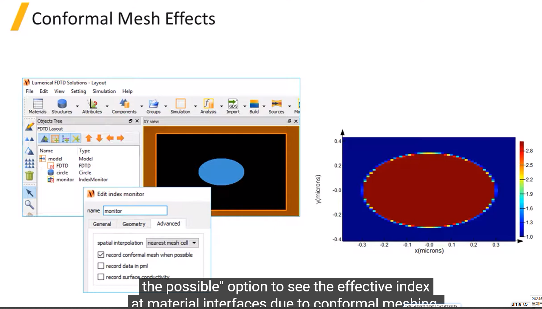
So using an index monitor can be helpful to confirm that the mesh is set up with the correct mesh size. To achieve this, add a refractive index monitor from the monitor Yours drop down menu. Edit monitor using the Edit button or E keyboard shortcuts for the index monitor.
Since the number of frequency points recorded is one by default, you can see that the override Global monitor settings is overwritten by default Using one frequency point here is fine since the structure that we're simulating is a dielectric material, which means that the refracted index doesn't change on function of frequency in the geometry tab, the monitor type is 2D z normal, which means we'll get the refractive index and the xy plane at a particular Z position set the size of the index mode to match the size of the simulation region, which is 2.5 microns in the x and y directions, and set the Z position to zero, which corresponds with the center position of the slab click OK to visit the settings in the viewport.
As you can see, the yellow outline of the monitor with the monitor selected, the available preview OFS are listed and then the result? Right click to view the index preview. This doesn't support the automatic unfolding of the monitor data across symmetry boundaries. So you can see that we can only see one quarter of the structure from the color bar scale scale. On the right, you can see that the slab has a refractive index of 2.65, and the etched holes have a refractive index of one.
As expected, we can also see that the shape of the etched holes in each period is the same, which is what we wanted back.
Now run the simulation, then plot the refractive index result. This result does apply the unfolding across the symmetry of boundaries so that we can see the full refractive index cross section. Now that we've seen an example of setting up the index monitor, here are some tips for using the monitor.
You may find that if there are many small features of the structure, There can be some graphical artifacts in the plot, so it's best to zoom into the plot, but by using the Zoom mouse mode and clicking on or selecting a region of the plot to zoom into to clearly see the material, little interfaces of the structure index monitors may not accurately record material properties in regions using advanced nonlinear material models or Gra attributes, you can use the nearest mesh cell interpolation option with the record controlled mesh when possible option to see the effective index at material interfaces due to conformal meshing, you'll only see this once the structure has been ached after running this simulation, so you won't see this on the index preview if you want to get this result without running the full simulation, you can use either the quit and save in the job integer after the changing stages, the simulation has become completed and the simulator is the running stage.
The spatial interpolation options are advanced features, so we recommend changing positions as directly by numerical staff.
指数监视器返回折射指数或表面电导率分布。
这个监视器可以有2D或3D几何图形,默认情况下,它只返回一个频点的结果。此监视器最常用于检查将要模拟的结构,以确保其设置正确。 如果你有一个由许多不同物体组成的复杂结构,它就特别有用。
如果您有多个重叠的对象,它也会很有帮助,因为它允许您检查重叠区域中将模拟哪个对象。网格顺序较低的对象将优先处理。有关重叠对象的网格顺序和网格划分优先级的更多信息,请参见下面的页面链接。另一种情况是,如果你有一个折射率随空间函数而变化的结构,指数监视器可以让你检查得到的折射率分布。大多数监视器数据仅在运行相同的模拟后才可用。
但是,在运行模拟之前,可以预览折射率分布和表面电导率。必须先添加模拟区域,然后才能生成索引数据预览。
绘制预览图可用作在运行仿真之前检查仿真结构的快速方法。来自指数监视器的数据也用于计算各种量,例如空间功率吸收和光学发生速率。常见的后处理数据分析函数可以在对象库的分析部分找到。
另一种情况是,如果你有一个具有折射率的结构,它会随着空间的函数而变化,指数监视器可以让你检查得到的折射率分布。
这个文件包含一个光子晶体谐振腔,它是一个比周围介质具有更高折射指数的平板。所述空腔是通过在空腔中心周围蚀刻一组孔而形成的。在模拟区域中,在X和Y方向上使用了对称性,以减少光子晶体结构的存储需求。结构的周期性可能很重要,因此确保每个网格孔的形状在图案的每个周期中都是相同的非常重要。
使用折射率监视器有助于确认网格是否设置了正确的网格尺寸
因此,使用折射率监视器有助于确认网格是否设置了正确的网格尺寸。要实现这一点,请从显示器下拉菜单中添加一个折射率监测器。使用 “编辑” 按钮或键盘快捷方式编辑索引监视器。
由于默认记录的频点数为1,因此您可以看到默认使用一个覆盖全局监视器设置覆盖,频点在这里很好,因为我们模拟的结构是介电材料,这意味着折射指数不会在几何选项卡中的频率函数上发生变化,监视器类型为2D z法线,这意味着我们将获取特定Z位置的折射率和xy平面,设置索引模式的大小以匹配模拟区域的大小,即x和y方向上的2.5微米,并将Z位置设置为零,这与平板的中心位置相对应,单击 “确定” 以访问视口中的设置。
正如您所看到的,选择了监视器的黄色轮廓,列出了可用的预览,然后是结果?右键单击以查看索引预览。这不支持监视器数据跨对称边界自动展开。因此,您可以看到我们只能从色条刻度中看到结构的四分之一。在右边,你可以看到平板的折射率为2.65,而蚀刻的孔的折射率为1。
正如预期的那样,我们还可以看到每个时期中蚀刻孔的形状都是相同的,这正是我们想要的。
现在运行模拟,然后绘制折射率结果。这个结果确实适用于跨越边界对称性的展开,以便我们可以看到完整的折射率横截面。现在我们已经看到了设置索引监视器的示例,这里有一些使用监视器的技巧。
您可能会发现,如果结构有许多小特征,则绘图中可能会有一些图形工件,因此最好放大绘图,但是通过使用缩放鼠标模式并单击或选择要放大的绘图区域以清楚地看到材料。
结构指数监测器的小接口可能无法使用高级非线性材料模型或Gra属性准确记录区域中的材料属性,您可以使用最近的网格单元插值选项和记录控制网格 (如果可能) 选项,以查看由于保角网格划分导致的材料接口的有效索引。只有在运行此模拟后缓存结构后,您才会看到这一点,因此如果您想在不运行完整模拟的情况下获得此结果,您将不会在索引预览中看到这一点,您可以在更改阶段后使用退出并保存在作业整数中,模拟已经完成,模拟器是运行阶段。【就是运行起来之后,点quit and save,然后点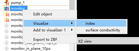
来查看折射率的分布!当我在mesh中网格设置为16.6667nm时,结果发现,我设置的200nm厚度z方向,但实际上是108x2nm!
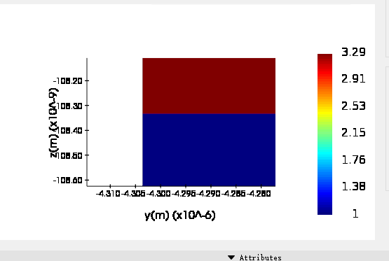
偏差特别大!【我已经设置了z方向网格整除(因为200/16.6667约等于12,但依然会有这么大的偏差,很奇怪!!!后来发现原因是:
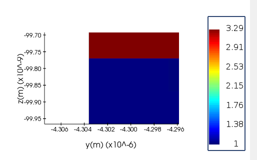
我其实之前一段时间计算的dz=16.4nm情况,对应的折射率分布: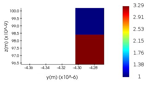
,z方向和200相比,只相差3nm. 误差很小。
而若dz=16.6667,则对应的折射率分布可以看出,z方向最大变成了108nm,和200相比,相差了16nm,导致误差非常大。
若dz=16.66,则就依然是200nm: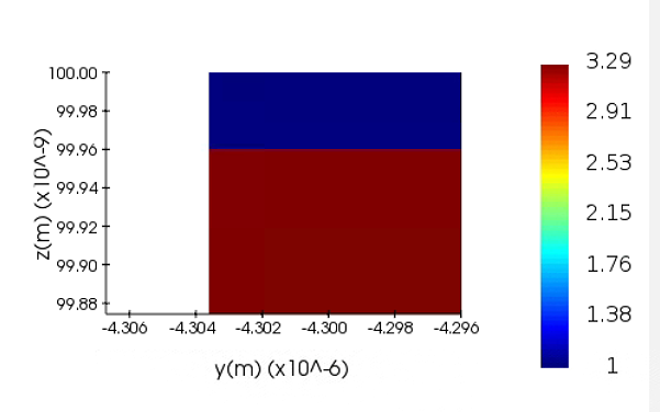
综上,fdtd不能识别小数点后三位!!!所以导致误差特别大。应设为16.66,然后用折射率监视器看一下是否200nm
】
】
空间插值选项是高级功能,因此我们建议直接通过数值人员更改位置。
FDTD自动划分的网格不可信!!!需要用折射率监视器preview一下,非常关键,否则计算出的波长有问题!!!和comsol对不上。所以以后必须进行这一步
我在网上查了,确实有人说运行模型之前除了检查材料拟合、内存、resource,还有折射率监视器!
李师兄说,他用FDTD无源仿真得到的波长与comsol无源仿真得到的波长不一致,就是因为用折射率监视器preview一下,发现z方向不是设置的200nm,而是216nm,他说他通过调节mesh,让折射率监视器也显示z方向厚度为200nm时,fdtd和comsol无源仿真的波长就能对上了。
刘师姐说:老师以前把官网的有源的激光器模型下载下来,有源仿真跑了一下,然后无源仿真跑了一下(就是不用四能级两电子材料而已),有源仿真和无源仿真的波长结果也不一样的!所以:
对FDTD软件,有源仿真和无源仿真得到的波长结果就是不一样,是没办法的!!!。然而张师兄论文和马仁敏nature等,就是用comsol无源仿真算的,能和实验对上。不知道为什么。算了
对我的模型,通过不断调dz到16.66nm时,发现dz设为16.66nm时,折射率监视器显示板子厚度就是200nm了!!!
运行之前preview一下:
此时z方向网格被没有整除,是正常的吧: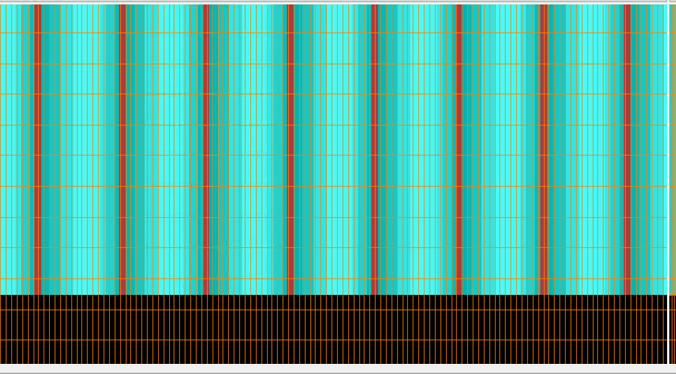
- 出现以上问题的原因:可能是网格对折射率进行了一些平均 啥的。
有人也遇到过:https://innovationspace.ansys.com/forum/forums/reply/147383/
问题:在lumerical fdtd软件中,lumerical fdtd 网格不能跨越两个材料之间的界面吗?必须dz设置为材料厚度的整除因子吗?为什么?材料厚度为200nm,可是当我将dz设为厚度的整除因子10nm时,从折射率监视器来看折射率,显示厚度为210nm,多了10nm. 若我将dz设为16.66,则折射率监视器显示厚度为200nm,但网格跨越了两个材料之间的界面。所以到底是以折射率监视器为准,还是以"网格不能跨越两个材料之间的界面"为准来设置dz? 请广泛查阅中英文资料,然后用中文仔细回复
- 没标准答案,问GPT后,我的答案:当dz比较小时,就以折射率监视器为准。当dz较大时,就还是不要跨越材料界面为准。【因为dz较大时,跨界面影响很大,而dz较小时,跨界面这件事影响很小,因为在官网https://optics.ansys.com/hc/en-us/articles/360034382614-Selecting-the-best-mesh-refinement-option-in-the-FDTD-simulation-object 提到:"在 400-1000 nm 的波长范围内使用每个波长 10 个点的网格分辨率进行测试。这个简单的测试演示了 CMT 解析子单元特征的能力,在本例中,子单元特征是不一定与离散网格匹配的界面的位置。 测试表明,在每波长 10 点的网格分辨率下,CMT 提供的精度明显高于在每波长 34 点的网格分辨率下获得的阶梯结果。" 和 "有关更多信息,请参阅下面的共形网格技术详细信息。如果在单个单元中发现两种以上材料,则该方法将恢复为该单元的阶梯法。阶梯:评估 Yee 单元每个位置的材质以确定其所在的材质,并且该位置的 E 场仅使用该单一材质属性。由此产生的离散结构无法解释任何单个 Yee 单元内发生的结构变化,从而导致与笛卡尔网格一致的“阶梯”介电常数网格此外,任何层都会有效地移动到 Yee 单元上最近的 E 场位置,这意味着层厚度无法解析为优于 dx。
"
Lumerical 的默认网格生成采用保形网格技术 (Conformal Mesh Technology, CMT),这可以更精确地处理材料界面,从而避免因网格跨越材料界面而引入的误差。
】 - 在https://innovationspace.ansys.com/courses/courses/lumerical-fdtd-monitors/lessons/index-monitor-in-ansys-lumerical-fdtd-lesson-2/?template=discovery 中提到折射率监视器可以看网格。
- 总之,最后峰值波长有四五nm误差也正常吧。
我的有源仿真计算结果显示"当z方向都整除时(分别使用5nm和10nm的dz,它们的区别只有折射率监视器的厚度分别是205和210nm),结果多模峰值波长也整体都偏差5、6、7nm等,所以折射率监视器厚度很重要。另外,当z方向折射率监视器厚度都一样时,dz分别为16.4和16.66nm,它们的区别只有z方向跨越了界面,且跨越高度不一样,结果多模峰值波长也整体都偏差5、6nm等,所以z方向有没有跨越界面也很重要。""因此综上,就应该同时满足z方向网格整除(网格没跨越界面) 以及 折射率监视器厚度一致!!!
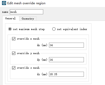
11.26更新:重大发现:可以在z方向设置三个mesh网格(界面两个),从而既满足z方向整除dz,又满足折射率监视器为200nm,以后都这样做!!!
一共z方向三个网格:中间这个网格dz=16nm: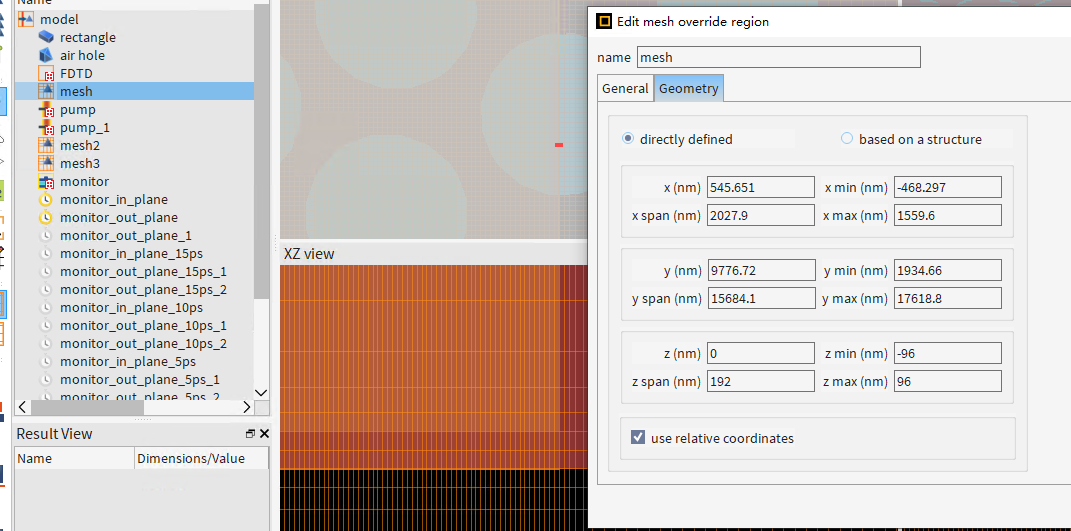
界面处的两个网格dz=2nm: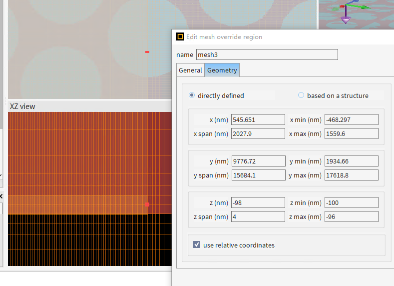
这样刚好dz整除,网格没有跨越界面,且折射率监视器显示才202nm,可以了!
- 但后面运行发现这样需要40小时才能算出来,太慢了。所以:
三个网格在z方向分别设为dz=12nm,dz=16nm,dz=12nm,但厚度又变成212nm. 权衡后选dz=5, 15,5nm
还有一种方法就是将几何结构中材料厚度设为195nm,然后三个网格在z方向分别设为dz=5(两份),15,5nm. 这样就既满足了折射率监视器200nm,又满足了网格不跨越界面!
问gpt知道的。
fdtd官网说,网格应设置:Mesh的典型应用是dx=dy<lamda/(10n),n是材料中的最高折射率
Mesh的典型应用是dx=dy<lamda/(10n),n是材料中的最高折射率
来自:https://mp.weixin.qq.com/s/sO749dzqwFBAPUDppWaAJw
但有源仿真可能不是,还需要迭代网格


【推荐】国内首个AI IDE,深度理解中文开发场景,立即下载体验Trae
【推荐】编程新体验,更懂你的AI,立即体验豆包MarsCode编程助手
【推荐】抖音旗下AI助手豆包,你的智能百科全书,全免费不限次数
【推荐】轻量又高性能的 SSH 工具 IShell:AI 加持,快人一步
· 10年+ .NET Coder 心语 ── 封装的思维:从隐藏、稳定开始理解其本质意义
· 地球OL攻略 —— 某应届生求职总结
· 提示词工程——AI应用必不可少的技术
· Open-Sora 2.0 重磅开源!
· 周边上新:园子的第一款马克杯温暖上架