
(原創) 如何解決warning:『PLL output port feeds output pin via non-dedicated routing -- jitter performance depends on switching rate of other design elements. Use PLL dedicated clock outputs to ensure jitter performance』? (SOC) (Quartus II) (DE2-70)
 無論是自己開發的project,或者是DE2-70 CD上的範例,只要Quartus II編譯後,幾乎大家都會遇到這個warning,到底是什麼意思呢?該如何解決這個warning呢?
Abstract
無論是自己開發的project,或者是DE2-70 CD上的範例,只要Quartus II編譯後,幾乎大家都會遇到這個warning,到底是什麼意思呢?該如何解決這個warning呢?
Introduction
使用環境:Quartus II 8.1+ DE2-70 (Cyclone II EP2C70F896C6N)
小美與阿帥在(原創) 如何使用Pipeline Bridge增進Nios II系統的Fmax? (SOC) (Quartus II) (Nios II) (SOPC Builder) (DE2-70)成功解掉1個critical warning後,也開始對Quartus II其他warning感興趣,基本上大部分的warning的意義都很明確,也都能解掉,但對於以下這個warning,阿帥卡了很久還是解不掉:

查了一下Quartus II 8.1的Help,這是Altera的官方回答
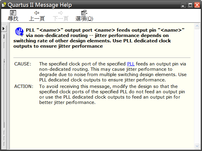
並不是英文看不懂,只是看來看去,還是不知道該怎麼解決,最後小美與阿帥打算去請教無雙學長。
『小美與阿帥不錯喔,已經會開始注意Quartus II的warning了!!』
『哈哈哈,深入研究才發現,其實Quartus II warning很多都是蠻貼心的警告,就像寫Visual C++與gcc時,都會盡量讓warning不要出現,所以現在也希望盡量能解掉Quartus II的warning』阿帥很自豪的回答。
『這樣的習慣不錯,這樣會讓你更了解Quartus II在做什麼。』不過無雙學長話鋒一轉『你問的這個問題,其實也困擾我很久,因為找不到解決方法,又暫時不影響結果,就先擱在一旁不管了,今天你又問起,我又仔細的研究了一番。』
『在Altera Forum有人討論過這個問題http://www.alteraforum.com/forum/showthread.php?t=1104,Ben與Brad講解的很清楚,你們兩個待會可以仔細閱讀他們的解釋,大至上的意思是說:由pll產生的clk,要ouput到專屬提供pll ouput的port,若output到非專屬pll output的port,Quartus II就會產生這個warning。』
『這樣好抽像喔,學長可以講的更清楚些嗎?』小美有聽沒有懂,還是滿臉疑惑。
『就用你們寫的code來講解好了...』
DE2_70.v / Verilog
2 (C) OOMusou 2008 http://oomusou.cnblogs.com
3
4 Filename : DE2_70.v
5 Compiler : Quartus II 8.1
6 Description : Demo how to use TRDB-D5M with LTM on DE2-70 with Nios II
7 Release : 12/18/2008 1.0
8 */
9
10 `default_nettype none
11
12 module DE2_70 (
13 //////////////////////// Clock Input ////////////////////////
14 input iCLK_28, // 28.63636 MHz
15 input iCLK_50, // 50 MHz
16 input iCLK_50_2, // 50 MHz
17 input iCLK_50_3, // 50 MHz
18 input iCLK_50_4, // 50 MHz
19 input iEXT_CLOCK, // External Clock
20 //////////////////////// Push Button ////////////////////////
21 input [3:0] iKEY, // Pushbutton[3:0]
22 //////////////////////// DPDT Switch ////////////////////////
23 input [17:0] iSW, // Toggle Switch[17:0]
24 //////////////////////// 7-SEG Dispaly ////////////////////////
25 output [6:0] oHEX0_D, // Seven Segment Digit 0
26 output [6:0] oHEX1_D, // Seven Segment Digit 1
27 output [6:0] oHEX2_D, // Seven Segment Digit 2
28 output [6:0] oHEX3_D, // Seven Segment Digit 3
29 output [6:0] oHEX4_D, // Seven Segment Digit 4
30 output [6:0] oHEX5_D, // Seven Segment Digit 5
31 output [6:0] oHEX6_D, // Seven Segment Digit 6
32 output [6:0] oHEX7_D, // Seven Segment Digit 7
33 //////////////////////////// LED ////////////////////////////
34 output [8:0] oLEDG, // LED Green[8:0]
35 output [17:0] oLEDR, // LED Red[17:0]
36 /////////////////////// SDRAM Interface ////////////////////////
37 inout [31:0] DRAM_DQ, // SDRAM Data bus 32 Bits
38 output [12:0] oDRAM0_A, // SDRAM0 Address bus 13 Bits
39 output [12:0] oDRAM1_A, // SDRAM1 Address bus 13 Bits
40 output oDRAM0_LDQM0, // SDRAM0 Low-byte Data Mask
41 output oDRAM1_LDQM0, // SDRAM1 Low-byte Data Mask
42 output oDRAM0_UDQM1, // SDRAM0 High-byte Data Mask
43 output oDRAM1_UDQM1, // SDRAM1 High-byte Data Mask
44 output oDRAM0_WE_N, // SDRAM0 Write Enable
45 output oDRAM1_WE_N, // SDRAM1 Write Enable
46 output oDRAM0_CAS_N, // SDRAM0 Column Address Strobe
47 output oDRAM1_CAS_N, // SDRAM1 Column Address Strobe
48 output oDRAM0_RAS_N, // SDRAM0 Row Address Strobe
49 output oDRAM1_RAS_N, // SDRAM1 Row Address Strobe
50 output oDRAM0_CS_N, // SDRAM0 Chip Select
51 output oDRAM1_CS_N, // SDRAM1 Chip Select
52 output [1:0] oDRAM0_BA, // SDRAM0 Bank Address
53 output [1:0] oDRAM1_BA, // SDRAM1 Bank Address
54 output oDRAM0_CLK, // SDRAM0 Clock
55 output oDRAM1_CLK, // SDRAM1 Clock
56 output oDRAM0_CKE, // SDRAM0 Clock Enable
57 output oDRAM1_CKE, // SDRAM1 Clock Enable
58 //////////////////////// Flash Interface ////////////////////////
59 inout [14:0] FLASH_DQ, // FLASH Data bus 15 Bits (0 to 14)
60 inout FLASH_DQ15_AM1, // FLASH Data bus Bit 15 or Address A-1
61 output [21:0] oFLASH_A, // FLASH Address bus 26 Bits
62 output oFLASH_WE_N, // FLASH Write Enable
63 output oFLASH_RST_N, // FLASH Reset
64 output oFLASH_WP_N, // FLASH Write Protect /Programming Acceleration
65 input iFLASH_RY_N, // FLASH Ready/Busy output
66 output oFLASH_BYTE_N, // FLASH Byte/Word Mode Configuration
67 output oFLASH_OE_N, // FLASH Output Enable
68 output oFLASH_CE_N, // FLASH Chip Enable
69 //////////////////////// SRAM Interface ////////////////////////
70 inout [31:0] SRAM_DQ, // SRAM Data Bus 32 Bits
71 inout [3:0] SRAM_DPA, // SRAM Parity Data Bus
72 output [18:0] oSRAM_A, // SRAM Address bus 21 Bits
73 output oSRAM_ADSC_N, // SRAM Controller Address Status
74 output oSRAM_ADSP_N, // SRAM Processor Address Status
75 output oSRAM_ADV_N, // SRAM Burst Address Advance
76 output [3:0] oSRAM_BE_N, // SRAM Byte Write Enable
77 output oSRAM_CE1_N, // SRAM Chip Enable
78 output oSRAM_CE2, // SRAM Chip Enable
79 output oSRAM_CE3_N, // SRAM Chip Enable
80 output oSRAM_CLK, // SRAM Clock
81 output oSRAM_GW_N, // SRAM Global Write Enable
82 output oSRAM_OE_N, // SRAM Output Enable
83 output oSRAM_WE_N, // SRAM Write Enable
84 //////////////////////// GPIO ////////////////////////////////
85 inout [31:0] GPIO_0, // GPIO Connection 0 I/O
86 input GPIO_CLKIN_N0, // GPIO Connection 0 Clock Input 0
87 input GPIO_CLKIN_P0, // GPIO Connection 0 Clock Input 1
88 inout GPIO_CLKOUT_N0, // GPIO Connection 0 Clock Output 0
89 inout GPIO_CLKOUT_P0, // GPIO Connection 0 Clock Output 1
90 inout [31:0] GPIO_1, // GPIO Connection 1 I/O
91 input GPIO_CLKIN_N1, // GPIO Connection 1 Clock Input 0
92 input GPIO_CLKIN_P1, // GPIO Connection 1 Clock Input 1
93 inout GPIO_CLKOUT_N1, // GPIO Connection 1 Clock Output 0
94 inout GPIO_CLKOUT_P1, // GPIO Connection 1 Clock Output 1
95 //////////////////// SD Card Interface ////////////////////////
96 inout SD_DAT, // SD Card Data
97 inout SD_DAT3, // SD Card Data 3
98 inout SD_CMD, // SD Card Command Signal
99 output oSD_CLK // SD Card Clock
100 );
101
102 // ltm
103 wire [7:0] ltm_r; // ltm red data 8 bits
104 wire [7:0] ltm_g; // ltm green data 8 bits
105 wire [7:0] ltm_b; // ltm blue data 8 bits
106 wire ltm_nclk; // ltm clcok
107 wire ltm_hd; // ltm h.sync
108 wire ltm_vd; // ltm v.sync
109 wire ltm_den; // ltm data enable
110
111 // ltm config
112 wire ltm_sclk; // ltm I2S clk
113 wire ltm_scen; // ltm I2s clk enable
114 wire adc_ltm_sclk; // acd_ltm I2s clk enable
115 wire ltm_grst; // ltm reset
116
117 assign ltm_grst = iKEY[0]; // ltm rest
118 assign adc_ltm_sclk = ltm_sclk; // ltm i2s clk enable
119 assign GPIO_0[2] = adc_ltm_sclk; // acd_ltm i2sclk enable
120 assign GPIO_0[3] = ltm_b[3]; // ltm blue data 8 bits
121 assign GPIO_0[4] = ltm_b[2]; // ltm blue data 8 bits
122 assign GPIO_0[5] = ltm_b[1]; // ltm blue data 8 bits
123 assign GPIO_0[6] = ltm_b[0]; // ltm blue data 8 bits
124 assign GPIO_0[7] =~ltm_nclk; // ltm clcok
125 assign GPIO_0[8] = ltm_den; // ltm data enable
126 assign GPIO_0[9] = ltm_hd; // ltm h.sync
127 assign GPIO_0[10] = ltm_vd; // ltm v.sync
128 assign GPIO_0[11] = ltm_b[4]; // ltm blue data 8 bits
129 assign GPIO_0[12] = ltm_b[5]; // ltm blue data 8 bits
130 assign GPIO_0[13] = ltm_b[6]; // ltm blue data 8 bits
131 assign GPIO_CLKOUT_N0 = ltm_b[7]; // ltm blue data 8 bits
132 assign GPIO_0[14] = ltm_g[0]; // ltm blue data 8 bits
133 assign GPIO_CLKOUT_P0 = ltm_g[1]; // ltm blue data 8 bits
134 assign GPIO_0[15] = ltm_g[2]; // ltm blue data 8 bits
135 assign GPIO_0[16] = ltm_g[3]; // ltm blue data 8 bits
136 assign GPIO_0[17] = ltm_g[4]; // ltm blue data 8 bits
137 assign GPIO_0[18] = ltm_g[5]; // ltm blue data 8 bits
138 assign GPIO_0[19] = ltm_g[6]; // ltm blue data 8 bits
139 assign GPIO_0[20] = ltm_g[7]; // ltm blue data 8 bits
140 assign GPIO_0[21] = ltm_r[0]; // ltm red data 8 bits
141 assign GPIO_0[22] = ltm_r[1]; // ltm red data 8 bits
142 assign GPIO_0[23] = ltm_r[2]; // ltm red data 8 bits
143 assign GPIO_0[24] = ltm_r[3]; // ltm red data 8 bits
144 assign GPIO_0[25] = ltm_r[4]; // ltm red data 8 bits
145 assign GPIO_0[26] = ltm_r[5]; // ltm red data 8 bits
146 assign GPIO_0[27] = ltm_r[6]; // ltm red data 8 bits
147 assign GPIO_0[28] = ltm_r[7]; // ltm red data 8 bits
148 assign GPIO_0[29] = ltm_grst; // ltm red data 8 bits
149 assign GPIO_0[30] = ltm_scen; // ltm sclk enable
150
151 // reset_delay
152 wire dly_rst_0; // reset delay 0
153 wire dly_rst_1; // reset delay 1
154 wire dly_rst_2; // reset delay 2
155
156 Reset_Delay reset0 (
157 .iCLK(iCLK_50), // 50 MHz
158 .iRST(iKEY[0]), // Pushbutton[0]
159 .oRST_0(dly_rst_0), // reset delay 0
160 .oRST_1(dly_rst_1), // reset delay 1
161 .oRST_2(dly_rst_2) // reset delay 2
162 );
163
164 // flash
165 wire flash_16bit_ip_a0;
166
167 assign oFLASH_BYTE_N = 1'b1; // flash byte/word mode configuration
168 assign oFLASH_RST_N = 1'b1; // flash reset
169 assign oFLASH_WP_N = 1'b1; // flash write protect /programming acceleration
170
171 // ssram
172 wire sram_clk; // sram clock
173 wire [1:0] sram_dummy_addr; // used to ignore the a0/a1 pin from cypress ssram ip core
174 wire sram_dummy_addr0; // used to ignore msb of sram address
175
176 assign oSRAM_CLK = sram_clk; // sram clock
177 assign oSRAM_A[18] = 1'bz; // ignore oSRAM_A[18]
178 assign oSRAM_ADSP_N = 1'b1; // sram processor address status
179 assign oSRAM_ADV_N = 1'b1; // sram burst address advance
180 assign oSRAM_CE2 = ~oSRAM_CE1_N; // sram chip enable
181 assign oSRAM_CE3_N = oSRAM_CE1_N; // sram chip enable
182 assign oSRAM_GW_N = 1'b1; // sram global write enable
183
184 // sdram (dual channel)
185 // the sdram is shared with Hw and SW
186 wire [12:0] dram_a; // sdram address
187 wire [1:0] dram_ba; // sdram bank address
188 wire dram_cas_n; // sdram column address strobe
189 wire dram_cke; // sdram clock enable
190 wire dram_cs_n; // sdram chip select
191 wire [3:0] dram_dqm; // sdram data mask
192 wire dram_ras_n; // sdram row address strobe
193 wire dram_we_n; // sdram write enable
194
195 // sdram0
196 assign oDRAM0_CLK = sram_clk; // sdram0 clock
197 assign oDRAM0_A = dram_a; // sdram0 address bus 13 bits
198 assign oDRAM0_BA = dram_ba; // sdram0 bank address
199 assign oDRAM0_CAS_N = dram_cas_n; // sdram0 column address strobe
200 assign oDRAM0_CKE = dram_cke; // sdram0 clock enable
201 assign oDRAM0_CS_N = dram_cs_n; // sdram0 chip select
202 assign oDRAM0_LDQM0 = dram_dqm[0]; // sdram0 low-byte data mask
203 assign oDRAM0_UDQM1 = dram_dqm[1]; // sdram0 high-byte data mask
204 assign oDRAM0_RAS_N = dram_ras_n; // sdram0 row address strobe
205 assign oDRAM0_WE_N = dram_we_n; // sdram0 write enable
206
207 // sdram1
208 assign oDRAM1_CLK = sram_clk; // sdram1 clock
209 assign oDRAM1_A = dram_a; // sdram1 clock
210 assign oDRAM1_BA = dram_ba; // sdram1 address bus 13 bits
211 assign oDRAM1_CAS_N = dram_cas_n; // sdram1 bank address
212 assign oDRAM1_CKE = dram_cke; // sdram1 column address strobe
213 assign oDRAM1_CS_N = dram_cs_n; // sdram1 clock enable
214 assign oDRAM1_LDQM0 = dram_dqm[2]; // sdram1 chip select
215 assign oDRAM1_UDQM1 = dram_dqm[3]; // sdram1 low-byte data mask
216 assign oDRAM1_RAS_N = dram_ras_n; // sdram1 high-byte data mask
217 assign oDRAM1_WE_N = dram_we_n; // sdram1 row address strobe
218 // sdram1 write enable
219
220 // LED
221 assign oLEDG[8] = 1'b0; // no use of ledg[8]
222 assign oLEDR[17:2] = 14'h0000; // no use of ledr[15:2]
223
224 // NIOS II CPU
225 wire cpu_clk; // cpu clk
226 wire cpu_reset_n; // cpu reset
227
228 assign cpu_reset_n = dly_rst_2; // cpu_reset
229
230 nios_ii nios0 (
231 // 1) global signals:
232 .clk_50(iCLK_50), // 50MHz
233 .pll_c0_system(cpu_clk), // cpu clk
234 .pll_c1_memory(sram_clk), // sram clk
235 .reset_n(cpu_reset_n), // cpu reset
236 // the_sdram
237 .zs_addr_from_the_sdram(dram_a), // sdram address
238 .zs_ba_from_the_sdram(dram_ba), // sdram bank address
239 .zs_cas_n_from_the_sdram(dram_cas_n), // sdram column address strobe
240 .zs_cke_from_the_sdram(dram_cke), // sdram clock enable
241 .zs_cs_n_from_the_sdram(dram_cs_n), // sdram chip select
242 .zs_dq_to_and_from_the_sdram(DRAM_DQ), // sdram data bus 32 bits
243 .zs_dqm_from_the_sdram(dram_dqm), // sdram data mask
244 .zs_ras_n_from_the_sdram(dram_ras_n), // sdram row address strobe
245 .zs_we_n_from_the_sdram(dram_we_n), // sdram write enable
246 // flash
247 .address_to_the_cfi_flash({oFLASH_A[21:0],flash_16bit_ip_a0}), // flash address bus 26 bits
248 .data_to_and_from_the_cfi_flash({FLASH_DQ15_AM1,FLASH_DQ}), // flash data bus 15 bits (0 to 14)
249 .read_n_to_the_cfi_flash(oFLASH_OE_N), // flash output enable
250 .select_n_to_the_cfi_flash(oFLASH_CE_N), // flash chip enable
251 .write_n_to_the_cfi_flash(oFLASH_WE_N), // flash write enable
252 // the_tristate_bridge_1_avalon_slave (ssram)
253 .address_to_the_ssram({sram_dummy_addr0, oSRAM_A[17:0],sram_dummy_addr}), // sram address bus 21 bits
254 .adsc_n_to_the_ssram(oSRAM_ADSC_N), // sram controller address status
255 .bw_n_to_the_ssram(oSRAM_BE_N), // sram byte write enable
256 .bwe_n_to_the_ssram(oSRAM_WE_N), // sram write enable
257 .chipenable1_n_to_the_ssram(oSRAM_CE1_N), // sram chip enable
258 .data_to_and_from_the_ssram((SRAM_DQ)), // sram data bus 32 bits
259 .outputenable_n_to_the_ssram(oSRAM_OE_N), // sram output enable
260 // the_ltm0
261 .coe_ltm_export_iCLK_50_to_the_ltm(iCLK_50_2), // 50MHz
262 .coe_ltm_export_iRST0_to_the_ltm(dly_rst_0), // reset delay 0
263 .coe_ltm_export_iRST2_to_the_ltm(dly_rst_2), // reset delay 2
264 .coe_ltm_export_oLTM_CLK_from_the_ltm(ltm_nclk), // ltm clcok
265 .coe_ltm_export_oR_from_the_ltm(ltm_r), // ltm red data 8 bits
266 .coe_ltm_export_oG_from_the_ltm(ltm_g), // ltm green data 8 bits
267 .coe_ltm_export_oB_from_the_ltm(ltm_b), // ltm blue data 8 bits
268 .coe_ltm_export_oHD_from_the_ltm(ltm_hd), // ltm h.sync
269 .coe_ltm_export_oVD_from_the_ltm(ltm_vd), // ltm v.sync
270 .coe_ltm_export_oDEN_from_the_ltm(ltm_den), // ltm data enable
271 .coe_ltm_export_oSCLK_from_the_ltm(ltm_sclk), // ltm sclk
272 .coe_ltm_export_ioSDAT_to_and_from_the_ltm(GPIO_0[31]), // ltm I2S data
273 .coe_ltm_export_oSCEN_from_the_ltm(ltm_scen), // ltm I2S clk enable
274 .coe_ltm_export_oFIFO_EMPTY_from_the_ltm(oLEDR[0]), // for debug use only (ltm fifo empty)
275 .coe_ltm_export_oFIFO_FULL_from_the_ltm(oLEDR[1]), // for debug use only (ltm fifo full)
276 // SD
277 .out_port_from_the_sd_clk(oSD_CLK), // SD Card Clock
278 .bidir_port_to_and_from_the_sd_cmd(SD_CMD), // SD Card Command Signal
279 .bidir_port_to_and_from_the_sd_dat(SD_DAT), // SD Card Data
280 .bidir_port_to_and_from_the_sd_dat3(SD_DAT3) // SD Card Data 3
281 );
282
283 endmodule
『234行的sram_clk,是由pll所產生的。』
// 1) global signals:
.clk_50(iCLK_50), // 50MHz
.pll_c0_system(cpu_clk), // cpu clk
.pll_c1_memory(sram_clk), // sram clk
『而Quartus II的warning,主要是來自於以下這幾行:』
176行
196行
208行
124行
『因為你將sram_clk這個由pll產生的clk output到oSRAM_CLK、oDRAM0_CLK、oDRAM1_CLK、GPIO_0[7]這些非pll專屬的output port,所以Quartus II才有以上這些warning?』
『DE2-70有這些pll專屬的output port嗎?』阿帥還是很懷疑。
『有,你看一下DE2-70 User Manual p.43,GPIO就有提供pll專屬的input與output port,Quartus II就是希望你pll產生的clk,能output到這種專屬的port以避免jitter。』
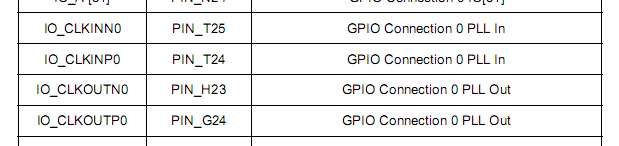
『可是在DE2-70上,SDRAM與SRAM都沒有專屬pll output port的設計怎麼辦?』小美仔細的查過DE2-70 User Manual,發現只有GPIO提供pll output port。
『對,這就牽涉到開發版的設計了,或許當初認為GPIO主要是外接自己的周邊,所以使用到pll的機會很大,因此設計了專屬的pll output port,不過在http://www.alteraforum.com/forum/showthread.php?t=1104中,Brad最後也做了結論,若你的clk port能接受pll的jitter的話,就可忽略這個warning。』
『那看來這個warning是解不掉了...』阿帥覺得有點失望...。
『雖然如此,也讓我們更了解Quartus II warning的意義,所以未嘗不是一件好事,畢竟只是warning,只要我們知道自己在幹什麼,能確保整個設計正常,就可放心的忽略這個warning。』無雙學長還是對小美與阿帥的研究精神加以肯定。
Conclusion
注意Quartus II warning是一個很好的習慣,就算可能不能完全解掉,但最少要知道這個warning在幹什麼。
See Also
(原創) 如何使用Pipeline Bridge增進Nios II系統的Fmax? (SOC) (Quartus II) (Nios II) (SOPC Builder) (DE2-70)
Reference
http://www.alteraforum.com/forum/showthread.php?t=1104
DE2-70 User Manual