

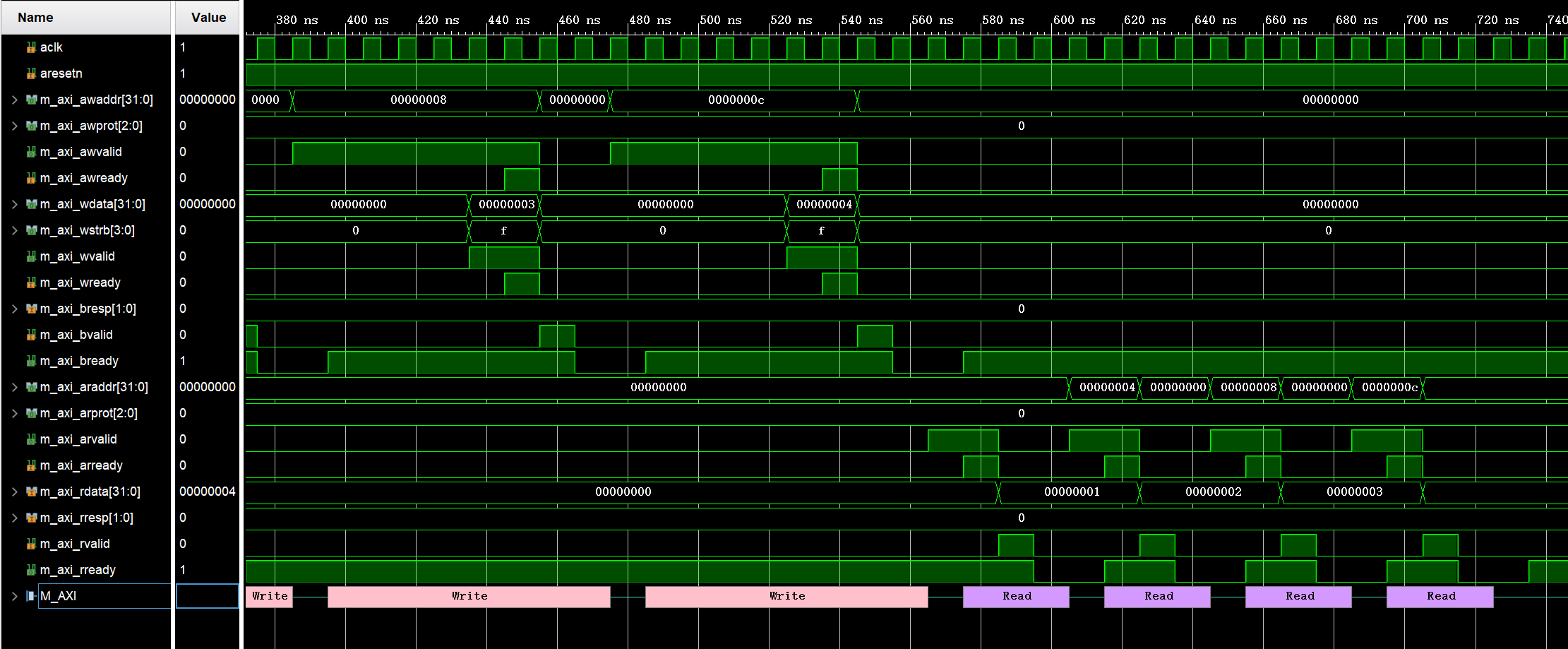
AXI lite总线读写时序
1. AXI_SLAVE源码
`timescale 1 ns / 1 ps

	module myip_v1_0_S00_AXI #
	(
		// Users to add parameters here

		// User parameters ends
		// Do not modify the parameters beyond this line

		// Width of S_AXI data bus
		parameter integer C_S_AXI_DATA_WIDTH	= 32,
		// Width of S_AXI address bus
		parameter integer C_S_AXI_ADDR_WIDTH	= 7
	)
	(
		// Users to add ports here

		// User ports ends
		// Do not modify the ports beyond this line

		// Global Clock Signal
		input wire  S_AXI_ACLK,
		// Global Reset Signal. This Signal is Active LOW
		input wire  S_AXI_ARESETN,
		// Write address (issued by master, acceped by Slave)
		input wire [C_S_AXI_ADDR_WIDTH-1 : 0] S_AXI_AWADDR,
		// Write channel Protection type. This signal indicates the
    		// privilege and security level of the transaction, and whether
    		// the transaction is a data access or an instruction access.
		input wire [2 : 0] S_AXI_AWPROT,
		// Write address valid. This signal indicates that the master signaling
    		// valid write address and control information.
		input wire  S_AXI_AWVALID,
		// Write address ready. This signal indicates that the slave is ready
    		// to accept an address and associated control signals.
		output wire  S_AXI_AWREADY,
		// Write data (issued by master, acceped by Slave)
		input wire [C_S_AXI_DATA_WIDTH-1 : 0] S_AXI_WDATA,
		// Write strobes. This signal indicates which byte lanes hold
    		// valid data. There is one write strobe bit for each eight
    		// bits of the write data bus.
		input wire [(C_S_AXI_DATA_WIDTH/8)-1 : 0] S_AXI_WSTRB,
		// Write valid. This signal indicates that valid write
    		// data and strobes are available.
		input wire  S_AXI_WVALID,
		// Write ready. This signal indicates that the slave
    		// can accept the write data.
		output wire  S_AXI_WREADY,
		// Write response. This signal indicates the status
    		// of the write transaction.
		output wire [1 : 0] S_AXI_BRESP,
		// Write response valid. This signal indicates that the channel
    		// is signaling a valid write response.
		output wire  S_AXI_BVALID,
		// Response ready. This signal indicates that the master
    		// can accept a write response.
		input wire  S_AXI_BREADY,
		// Read address (issued by master, acceped by Slave)
		input wire [C_S_AXI_ADDR_WIDTH-1 : 0] S_AXI_ARADDR,
		// Protection type. This signal indicates the privilege
    		// and security level of the transaction, and whether the
    		// transaction is a data access or an instruction access.
		input wire [2 : 0] S_AXI_ARPROT,
		// Read address valid. This signal indicates that the channel
    		// is signaling valid read address and control information.
		input wire  S_AXI_ARVALID,
		// Read address ready. This signal indicates that the slave is
    		// ready to accept an address and associated control signals.
		output wire  S_AXI_ARREADY,
		// Read data (issued by slave)
		output wire [C_S_AXI_DATA_WIDTH-1 : 0] S_AXI_RDATA,
		// Read response. This signal indicates the status of the
    		// read transfer.
		output wire [1 : 0] S_AXI_RRESP,
		// Read valid. This signal indicates that the channel is
    		// signaling the required read data.
		output wire  S_AXI_RVALID,
		// Read ready. This signal indicates that the master can
    		// accept the read data and response information.
		input wire  S_AXI_RREADY
	);

	// AXI4LITE signals
	reg [C_S_AXI_ADDR_WIDTH-1 : 0] 	axi_awaddr;
	reg  	axi_awready;
	reg  	axi_wready;
	reg [1 : 0] 	axi_bresp;
	reg  	axi_bvalid;
	reg [C_S_AXI_ADDR_WIDTH-1 : 0] 	axi_araddr;
	reg  	axi_arready;
	reg [C_S_AXI_DATA_WIDTH-1 : 0] 	axi_rdata;
	reg [1 : 0] 	axi_rresp;
	reg  	axi_rvalid;

	// Example-specific design signals
	// local parameter for addressing 32 bit / 64 bit C_S_AXI_DATA_WIDTH
	// ADDR_LSB is used for addressing 32/64 bit registers/memories
	// ADDR_LSB = 2 for 32 bits (n downto 2)
	// ADDR_LSB = 3 for 64 bits (n downto 3)
	localparam integer ADDR_LSB = (C_S_AXI_DATA_WIDTH/32) + 1;
	localparam integer OPT_MEM_ADDR_BITS = 4;
	//----------------------------------------------
	//-- Signals for user logic register space example
	//------------------------------------------------
	//-- Number of Slave Registers 20
	reg [C_S_AXI_DATA_WIDTH-1:0]	slv_reg0;
	reg [C_S_AXI_DATA_WIDTH-1:0]	slv_reg1;
	reg [C_S_AXI_DATA_WIDTH-1:0]	slv_reg2;
	reg [C_S_AXI_DATA_WIDTH-1:0]	slv_reg3;
	reg [C_S_AXI_DATA_WIDTH-1:0]	slv_reg4;
	reg [C_S_AXI_DATA_WIDTH-1:0]	slv_reg5;
	reg [C_S_AXI_DATA_WIDTH-1:0]	slv_reg6;
	reg [C_S_AXI_DATA_WIDTH-1:0]	slv_reg7;
	reg [C_S_AXI_DATA_WIDTH-1:0]	slv_reg8;
	reg [C_S_AXI_DATA_WIDTH-1:0]	slv_reg9;
	reg [C_S_AXI_DATA_WIDTH-1:0]	slv_reg10;
	reg [C_S_AXI_DATA_WIDTH-1:0]	slv_reg11;
	reg [C_S_AXI_DATA_WIDTH-1:0]	slv_reg12;
	reg [C_S_AXI_DATA_WIDTH-1:0]	slv_reg13;
	reg [C_S_AXI_DATA_WIDTH-1:0]	slv_reg14;
	reg [C_S_AXI_DATA_WIDTH-1:0]	slv_reg15;
	reg [C_S_AXI_DATA_WIDTH-1:0]	slv_reg16;
	reg [C_S_AXI_DATA_WIDTH-1:0]	slv_reg17;
	reg [C_S_AXI_DATA_WIDTH-1:0]	slv_reg18;
	reg [C_S_AXI_DATA_WIDTH-1:0]	slv_reg19;
	wire	 slv_reg_rden;
	wire	 slv_reg_wren;
	reg [C_S_AXI_DATA_WIDTH-1:0]	 reg_data_out;
	integer	 byte_index;
	reg	 aw_en;

	// I/O Connections assignments

	assign S_AXI_AWREADY	= axi_awready;
	assign S_AXI_WREADY	= axi_wready;
	assign S_AXI_BRESP	= axi_bresp;
	assign S_AXI_BVALID	= axi_bvalid;
	assign S_AXI_ARREADY	= axi_arready;
	assign S_AXI_RDATA	= axi_rdata;
	assign S_AXI_RRESP	= axi_rresp;
	assign S_AXI_RVALID	= axi_rvalid;
	// Implement axi_awready generation
	// axi_awready is asserted for one S_AXI_ACLK clock cycle when both
	// S_AXI_AWVALID and S_AXI_WVALID are asserted. axi_awready is
	// de-asserted when reset is low.

	always @( posedge S_AXI_ACLK )
	begin
	  if ( S_AXI_ARESETN == 1'b0 )
	    begin
	      axi_awready <= 1'b0;
	      aw_en <= 1'b1;
	    end
	  else
	    begin
	      if (~axi_awready && S_AXI_AWVALID && S_AXI_WVALID && aw_en)
	        begin
	          // slave is ready to accept write address when
	          // there is a valid write address and write data
	          // on the write address and data bus. This design
	          // expects no outstanding transactions.
	          axi_awready <= 1'b1;
	          aw_en <= 1'b0;
	        end
	        else if (S_AXI_BREADY && axi_bvalid)
	            begin
	              aw_en <= 1'b1;
	              axi_awready <= 1'b0;
	            end
	      else
	        begin
	          axi_awready <= 1'b0;
	        end
	    end
	end

	// Implement axi_awaddr latching
	// This process is used to latch the address when both
	// S_AXI_AWVALID and S_AXI_WVALID are valid.

	always @( posedge S_AXI_ACLK )
	begin
	  if ( S_AXI_ARESETN == 1'b0 )
	    begin
	      axi_awaddr <= 0;
	    end
	  else
	    begin
	      if (~axi_awready && S_AXI_AWVALID && S_AXI_WVALID && aw_en)
	        begin
	          // Write Address latching
	          axi_awaddr <= S_AXI_AWADDR;
	        end
	    end
	end

	// Implement axi_wready generation
	// axi_wready is asserted for one S_AXI_ACLK clock cycle when both
	// S_AXI_AWVALID and S_AXI_WVALID are asserted. axi_wready is
	// de-asserted when reset is low.

	always @( posedge S_AXI_ACLK )
	begin
	  if ( S_AXI_ARESETN == 1'b0 )
	    begin
	      axi_wready <= 1'b0;
	    end
	  else
	    begin
	      if (~axi_wready && S_AXI_WVALID && S_AXI_AWVALID && aw_en )
	        begin
	          // slave is ready to accept write data when
	          // there is a valid write address and write data
	          // on the write address and data bus. This design
	          // expects no outstanding transactions.
	          axi_wready <= 1'b1;
	        end
	      else
	        begin
	          axi_wready <= 1'b0;
	        end
	    end
	end

	// Implement memory mapped register select and write logic generation
	// The write data is accepted and written to memory mapped registers when
	// axi_awready, S_AXI_WVALID, axi_wready and S_AXI_WVALID are asserted. Write strobes are used to
	// select byte enables of slave registers while writing.
	// These registers are cleared when reset (active low) is applied.
	// Slave register write enable is asserted when valid address and data are available
	// and the slave is ready to accept the write address and write data.
	assign slv_reg_wren = axi_wready && S_AXI_WVALID && axi_awready && S_AXI_AWVALID;

	always @( posedge S_AXI_ACLK )
	begin
	  if ( S_AXI_ARESETN == 1'b0 )
	    begin
	      slv_reg0 <= 0;
	      slv_reg1 <= 0;
	      slv_reg2 <= 0;
	      slv_reg3 <= 0;
	      slv_reg4 <= 0;
	      slv_reg5 <= 0;
	      slv_reg6 <= 0;
	      slv_reg7 <= 0;
	      slv_reg8 <= 0;
	      slv_reg9 <= 0;
	      slv_reg10 <= 0;
	      slv_reg11 <= 0;
	      slv_reg12 <= 0;
	      slv_reg13 <= 0;
	      slv_reg14 <= 0;
	      slv_reg15 <= 0;
	      slv_reg16 <= 0;
	      slv_reg17 <= 0;
	      slv_reg18 <= 0;
	      slv_reg19 <= 0;
	    end
	  else begin
	    if (slv_reg_wren)
	      begin
	        case ( axi_awaddr[ADDR_LSB+OPT_MEM_ADDR_BITS:ADDR_LSB] )
	          5'h00:
	            for ( byte_index = 0; byte_index <= (C_S_AXI_DATA_WIDTH/8)-1; byte_index = byte_index+1 )
	              if ( S_AXI_WSTRB[byte_index] == 1 ) begin
	                // Respective byte enables are asserted as per write strobes
	                // Slave register 0
	                slv_reg0[(byte_index*8) +: 8] <= S_AXI_WDATA[(byte_index*8) +: 8];
	              end
	          5'h01:
	            for ( byte_index = 0; byte_index <= (C_S_AXI_DATA_WIDTH/8)-1; byte_index = byte_index+1 )
	              if ( S_AXI_WSTRB[byte_index] == 1 ) begin
	                // Respective byte enables are asserted as per write strobes
	                // Slave register 1
	                slv_reg1[(byte_index*8) +: 8] <= S_AXI_WDATA[(byte_index*8) +: 8];
	              end
	          5'h02:
	            for ( byte_index = 0; byte_index <= (C_S_AXI_DATA_WIDTH/8)-1; byte_index = byte_index+1 )
	              if ( S_AXI_WSTRB[byte_index] == 1 ) begin
	                // Respective byte enables are asserted as per write strobes
	                // Slave register 2
	                slv_reg2[(byte_index*8) +: 8] <= S_AXI_WDATA[(byte_index*8) +: 8];
	              end
	          5'h03:
	            for ( byte_index = 0; byte_index <= (C_S_AXI_DATA_WIDTH/8)-1; byte_index = byte_index+1 )
	              if ( S_AXI_WSTRB[byte_index] == 1 ) begin
	                // Respective byte enables are asserted as per write strobes
	                // Slave register 3
	                slv_reg3[(byte_index*8) +: 8] <= S_AXI_WDATA[(byte_index*8) +: 8];
	              end
	          5'h04:
	            for ( byte_index = 0; byte_index <= (C_S_AXI_DATA_WIDTH/8)-1; byte_index = byte_index+1 )
	              if ( S_AXI_WSTRB[byte_index] == 1 ) begin
	                // Respective byte enables are asserted as per write strobes
	                // Slave register 4
	                slv_reg4[(byte_index*8) +: 8] <= S_AXI_WDATA[(byte_index*8) +: 8];
	              end
	          5'h05:
	            for ( byte_index = 0; byte_index <= (C_S_AXI_DATA_WIDTH/8)-1; byte_index = byte_index+1 )
	              if ( S_AXI_WSTRB[byte_index] == 1 ) begin
	                // Respective byte enables are asserted as per write strobes
	                // Slave register 5
	                slv_reg5[(byte_index*8) +: 8] <= S_AXI_WDATA[(byte_index*8) +: 8];
	              end
	          5'h06:
	            for ( byte_index = 0; byte_index <= (C_S_AXI_DATA_WIDTH/8)-1; byte_index = byte_index+1 )
	              if ( S_AXI_WSTRB[byte_index] == 1 ) begin
	                // Respective byte enables are asserted as per write strobes
	                // Slave register 6
	                slv_reg6[(byte_index*8) +: 8] <= S_AXI_WDATA[(byte_index*8) +: 8];
	              end
	          5'h07:
	            for ( byte_index = 0; byte_index <= (C_S_AXI_DATA_WIDTH/8)-1; byte_index = byte_index+1 )
	              if ( S_AXI_WSTRB[byte_index] == 1 ) begin
	                // Respective byte enables are asserted as per write strobes
	                // Slave register 7
	                slv_reg7[(byte_index*8) +: 8] <= S_AXI_WDATA[(byte_index*8) +: 8];
	              end
	          5'h08:
	            for ( byte_index = 0; byte_index <= (C_S_AXI_DATA_WIDTH/8)-1; byte_index = byte_index+1 )
	              if ( S_AXI_WSTRB[byte_index] == 1 ) begin
	                // Respective byte enables are asserted as per write strobes
	                // Slave register 8
	                slv_reg8[(byte_index*8) +: 8] <= S_AXI_WDATA[(byte_index*8) +: 8];
	              end
	          5'h09:
	            for ( byte_index = 0; byte_index <= (C_S_AXI_DATA_WIDTH/8)-1; byte_index = byte_index+1 )
	              if ( S_AXI_WSTRB[byte_index] == 1 ) begin
	                // Respective byte enables are asserted as per write strobes
	                // Slave register 9
	                slv_reg9[(byte_index*8) +: 8] <= S_AXI_WDATA[(byte_index*8) +: 8];
	              end
	          5'h0A:
	            for ( byte_index = 0; byte_index <= (C_S_AXI_DATA_WIDTH/8)-1; byte_index = byte_index+1 )
	              if ( S_AXI_WSTRB[byte_index] == 1 ) begin
	                // Respective byte enables are asserted as per write strobes
	                // Slave register 10
	                slv_reg10[(byte_index*8) +: 8] <= S_AXI_WDATA[(byte_index*8) +: 8];
	              end
	          5'h0B:
	            for ( byte_index = 0; byte_index <= (C_S_AXI_DATA_WIDTH/8)-1; byte_index = byte_index+1 )
	              if ( S_AXI_WSTRB[byte_index] == 1 ) begin
	                // Respective byte enables are asserted as per write strobes
	                // Slave register 11
	                slv_reg11[(byte_index*8) +: 8] <= S_AXI_WDATA[(byte_index*8) +: 8];
	              end
	          5'h0C:
	            for ( byte_index = 0; byte_index <= (C_S_AXI_DATA_WIDTH/8)-1; byte_index = byte_index+1 )
	              if ( S_AXI_WSTRB[byte_index] == 1 ) begin
	                // Respective byte enables are asserted as per write strobes
	                // Slave register 12
	                slv_reg12[(byte_index*8) +: 8] <= S_AXI_WDATA[(byte_index*8) +: 8];
	              end
	          5'h0D:
	            for ( byte_index = 0; byte_index <= (C_S_AXI_DATA_WIDTH/8)-1; byte_index = byte_index+1 )
	              if ( S_AXI_WSTRB[byte_index] == 1 ) begin
	                // Respective byte enables are asserted as per write strobes
	                // Slave register 13
	                slv_reg13[(byte_index*8) +: 8] <= S_AXI_WDATA[(byte_index*8) +: 8];
	              end
	          5'h0E:
	            for ( byte_index = 0; byte_index <= (C_S_AXI_DATA_WIDTH/8)-1; byte_index = byte_index+1 )
	              if ( S_AXI_WSTRB[byte_index] == 1 ) begin
	                // Respective byte enables are asserted as per write strobes
	                // Slave register 14
	                slv_reg14[(byte_index*8) +: 8] <= S_AXI_WDATA[(byte_index*8) +: 8];
	              end
	          5'h0F:
	            for ( byte_index = 0; byte_index <= (C_S_AXI_DATA_WIDTH/8)-1; byte_index = byte_index+1 )
	              if ( S_AXI_WSTRB[byte_index] == 1 ) begin
	                // Respective byte enables are asserted as per write strobes
	                // Slave register 15
	                slv_reg15[(byte_index*8) +: 8] <= S_AXI_WDATA[(byte_index*8) +: 8];
	              end
	          5'h10:
	            for ( byte_index = 0; byte_index <= (C_S_AXI_DATA_WIDTH/8)-1; byte_index = byte_index+1 )
	              if ( S_AXI_WSTRB[byte_index] == 1 ) begin
	                // Respective byte enables are asserted as per write strobes
	                // Slave register 16
	                slv_reg16[(byte_index*8) +: 8] <= S_AXI_WDATA[(byte_index*8) +: 8];
	              end
	          5'h11:
	            for ( byte_index = 0; byte_index <= (C_S_AXI_DATA_WIDTH/8)-1; byte_index = byte_index+1 )
	              if ( S_AXI_WSTRB[byte_index] == 1 ) begin
	                // Respective byte enables are asserted as per write strobes
	                // Slave register 17
	                slv_reg17[(byte_index*8) +: 8] <= S_AXI_WDATA[(byte_index*8) +: 8];
	              end
	          5'h12:
	            for ( byte_index = 0; byte_index <= (C_S_AXI_DATA_WIDTH/8)-1; byte_index = byte_index+1 )
	              if ( S_AXI_WSTRB[byte_index] == 1 ) begin
	                // Respective byte enables are asserted as per write strobes
	                // Slave register 18
	                slv_reg18[(byte_index*8) +: 8] <= S_AXI_WDATA[(byte_index*8) +: 8];
	              end
	          5'h13:
	            for ( byte_index = 0; byte_index <= (C_S_AXI_DATA_WIDTH/8)-1; byte_index = byte_index+1 )
	              if ( S_AXI_WSTRB[byte_index] == 1 ) begin
	                // Respective byte enables are asserted as per write strobes
	                // Slave register 19
	                slv_reg19[(byte_index*8) +: 8] <= S_AXI_WDATA[(byte_index*8) +: 8];
	              end
	          default : begin
	                      slv_reg0 <= slv_reg0;
	                      slv_reg1 <= slv_reg1;
	                      slv_reg2 <= slv_reg2;
	                      slv_reg3 <= slv_reg3;
	                      slv_reg4 <= slv_reg4;
	                      slv_reg5 <= slv_reg5;
	                      slv_reg6 <= slv_reg6;
	                      slv_reg7 <= slv_reg7;
	                      slv_reg8 <= slv_reg8;
	                      slv_reg9 <= slv_reg9;
	                      slv_reg10 <= slv_reg10;
	                      slv_reg11 <= slv_reg11;
	                      slv_reg12 <= slv_reg12;
	                      slv_reg13 <= slv_reg13;
	                      slv_reg14 <= slv_reg14;
	                      slv_reg15 <= slv_reg15;
	                      slv_reg16 <= slv_reg16;
	                      slv_reg17 <= slv_reg17;
	                      slv_reg18 <= slv_reg18;
	                      slv_reg19 <= slv_reg19;
	                    end
	        endcase
	      end
	  end
	end

	// Implement write response logic generation
	// The write response and response valid signals are asserted by the slave
	// when axi_wready, S_AXI_WVALID, axi_wready and S_AXI_WVALID are asserted.
	// This marks the acceptance of address and indicates the status of
	// write transaction.

	always @( posedge S_AXI_ACLK )
	begin
	  if ( S_AXI_ARESETN == 1'b0 )
	    begin
	      axi_bvalid  <= 0;
	      axi_bresp   <= 2'b0;
	    end
	  else
	    begin
	      if (axi_awready && S_AXI_AWVALID && ~axi_bvalid && axi_wready && S_AXI_WVALID)
	        begin
	          // indicates a valid write response is available
	          axi_bvalid <= 1'b1;
	          axi_bresp  <= 2'b0; // 'OKAY' response
	        end                   // work error responses in future
	      else
	        begin
	          if (S_AXI_BREADY && axi_bvalid)
	            //check if bready is asserted while bvalid is high)
	            //(there is a possibility that bready is always asserted high)
	            begin
	              axi_bvalid <= 1'b0;
	            end
	        end
	    end
	end

	// Implement axi_arready generation
	// axi_arready is asserted for one S_AXI_ACLK clock cycle when
	// S_AXI_ARVALID is asserted. axi_awready is
	// de-asserted when reset (active low) is asserted.
	// The read address is also latched when S_AXI_ARVALID is
	// asserted. axi_araddr is reset to zero on reset assertion.

	always @( posedge S_AXI_ACLK )
	begin
	  if ( S_AXI_ARESETN == 1'b0 )
	    begin
	      axi_arready <= 1'b0;
	      axi_araddr  <= 32'b0;
	    end
	  else
	    begin
	      if (~axi_arready && S_AXI_ARVALID)
	        begin
	          // indicates that the slave has acceped the valid read address
	          axi_arready <= 1'b1;
	          // Read address latching
	          axi_araddr  <= S_AXI_ARADDR;
	        end
	      else
	        begin
	          axi_arready <= 1'b0;
	        end
	    end
	end

	// Implement axi_arvalid generation
	// axi_rvalid is asserted for one S_AXI_ACLK clock cycle when both
	// S_AXI_ARVALID and axi_arready are asserted. The slave registers
	// data are available on the axi_rdata bus at this instance. The
	// assertion of axi_rvalid marks the validity of read data on the
	// bus and axi_rresp indicates the status of read transaction.axi_rvalid
	// is deasserted on reset (active low). axi_rresp and axi_rdata are
	// cleared to zero on reset (active low).
	always @( posedge S_AXI_ACLK )
	begin
	  if ( S_AXI_ARESETN == 1'b0 )
	    begin
	      axi_rvalid <= 0;
	      axi_rresp  <= 0;
	    end
	  else
	    begin
	      if (axi_arready && S_AXI_ARVALID && ~axi_rvalid)
	        begin
	          // Valid read data is available at the read data bus
	          axi_rvalid <= 1'b1;
	          axi_rresp  <= 2'b0; // 'OKAY' response
	        end
	      else if (axi_rvalid && S_AXI_RREADY)
	        begin
	          // Read data is accepted by the master
	          axi_rvalid <= 1'b0;
	        end
	    end
	end

	// Implement memory mapped register select and read logic generation
	// Slave register read enable is asserted when valid address is available
	// and the slave is ready to accept the read address.
	assign slv_reg_rden = axi_arready & S_AXI_ARVALID & ~axi_rvalid;
	always @(*)
	begin
	      // Address decoding for reading registers
	      case ( axi_araddr[ADDR_LSB+OPT_MEM_ADDR_BITS:ADDR_LSB] )
	        5'h00   : reg_data_out <= slv_reg0;
	        5'h01   : reg_data_out <= slv_reg1;
	        5'h02   : reg_data_out <= slv_reg2;
	        5'h03   : reg_data_out <= slv_reg3;
	        5'h04   : reg_data_out <= slv_reg4;
	        5'h05   : reg_data_out <= slv_reg5;
	        5'h06   : reg_data_out <= slv_reg6;
	        5'h07   : reg_data_out <= slv_reg7;
	        5'h08   : reg_data_out <= slv_reg8;
	        5'h09   : reg_data_out <= slv_reg9;
	        5'h0A   : reg_data_out <= slv_reg10;
	        5'h0B   : reg_data_out <= slv_reg11;
	        5'h0C   : reg_data_out <= slv_reg12;
	        5'h0D   : reg_data_out <= slv_reg13;
	        5'h0E   : reg_data_out <= slv_reg14;
	        5'h0F   : reg_data_out <= slv_reg15;
	        5'h10   : reg_data_out <= slv_reg16;
	        5'h11   : reg_data_out <= slv_reg17;
	        5'h12   : reg_data_out <= slv_reg18;
	        5'h13   : reg_data_out <= slv_reg19;
	        default : reg_data_out <= 0;
	      endcase
	end

	// Output register or memory read data
	always @( posedge S_AXI_ACLK )
	begin
	  if ( S_AXI_ARESETN == 1'b0 )
	    begin
	      axi_rdata  <= 0;
	    end
	  else
	    begin
	      // When there is a valid read address (S_AXI_ARVALID) with
	      // acceptance of read address by the slave (axi_arready),
	      // output the read dada
	      if (slv_reg_rden)
	        begin
	          axi_rdata <= reg_data_out;     // register read data
	        end
	    end
	end

	// Add user logic here

	// User logic ends

	endmodule
2. AXI_MASTER源码
`timescale 1 ns / 1 ps

	module myip_v1_0_M00_AXI #
	(
		// Users to add parameters here

		// User parameters ends
		// Do not modify the parameters beyond this line

		// The master will start generating data from the C_M_START_DATA_VALUE value
		parameter  C_M_START_DATA_VALUE	= 32'hAA000000,
		// The master requires a target slave base address.
    // The master will initiate read and write transactions on the slave with base address specified here as a parameter.
		parameter  C_M_TARGET_SLAVE_BASE_ADDR	= 32'h40000000,
		// Width of M_AXI address bus.
    // The master generates the read and write addresses of width specified as C_M_AXI_ADDR_WIDTH.
		parameter integer C_M_AXI_ADDR_WIDTH	= 32,
		// Width of M_AXI data bus.
    // The master issues write data and accept read data where the width of the data bus is C_M_AXI_DATA_WIDTH
		parameter integer C_M_AXI_DATA_WIDTH	= 32,
		// Transaction number is the number of write
    // and read transactions the master will perform as a part of this example memory test.
		parameter integer C_M_TRANSACTIONS_NUM	= 4
	)
	(
		// Users to add ports here

		// User ports ends
		// Do not modify the ports beyond this line

		// Initiate AXI transactions
		input wire  INIT_AXI_TXN,
		// Asserts when ERROR is detected
		output reg  ERROR,
		// Asserts when AXI transactions is complete
		output wire  TXN_DONE,
		// AXI clock signal
		input wire  M_AXI_ACLK,
		// AXI active low reset signal
		input wire  M_AXI_ARESETN,
		// Master Interface Write Address Channel ports. Write address (issued by master)
		output wire [C_M_AXI_ADDR_WIDTH-1 : 0] M_AXI_AWADDR,
		// Write channel Protection type.
    // This signal indicates the privilege and security level of the transaction,
    // and whether the transaction is a data access or an instruction access.
		output wire [2 : 0] M_AXI_AWPROT,
		// Write address valid.
    // This signal indicates that the master signaling valid write address and control information.
		output wire  M_AXI_AWVALID,
		// Write address ready.
    // This signal indicates that the slave is ready to accept an address and associated control signals.
		input wire  M_AXI_AWREADY,
		// Master Interface Write Data Channel ports. Write data (issued by master)
		output wire [C_M_AXI_DATA_WIDTH-1 : 0] M_AXI_WDATA,
		// Write strobes.
    // This signal indicates which byte lanes hold valid data.
    // There is one write strobe bit for each eight bits of the write data bus.
		output wire [C_M_AXI_DATA_WIDTH/8-1 : 0] M_AXI_WSTRB,
		// Write valid. This signal indicates that valid write data and strobes are available.
		output wire  M_AXI_WVALID,
		// Write ready. This signal indicates that the slave can accept the write data.
		input wire  M_AXI_WREADY,
		// Master Interface Write Response Channel ports.
    // This signal indicates the status of the write transaction.
		input wire [1 : 0] M_AXI_BRESP,
		// Write response valid.
    // This signal indicates that the channel is signaling a valid write response
		input wire  M_AXI_BVALID,
		// Response ready. This signal indicates that the master can accept a write response.
		output wire  M_AXI_BREADY,
		// Master Interface Read Address Channel ports. Read address (issued by master)
		output wire [C_M_AXI_ADDR_WIDTH-1 : 0] M_AXI_ARADDR,
		// Protection type.
    // This signal indicates the privilege and security level of the transaction,
    // and whether the transaction is a data access or an instruction access.
		output wire [2 : 0] M_AXI_ARPROT,
		// Read address valid.
    // This signal indicates that the channel is signaling valid read address and control information.
		output wire  M_AXI_ARVALID,
		// Read address ready.
    // This signal indicates that the slave is ready to accept an address and associated control signals.
		input wire  M_AXI_ARREADY,
		// Master Interface Read Data Channel ports. Read data (issued by slave)
		input wire [C_M_AXI_DATA_WIDTH-1 : 0] M_AXI_RDATA,
		// Read response. This signal indicates the status of the read transfer.
		input wire [1 : 0] M_AXI_RRESP,
		// Read valid. This signal indicates that the channel is signaling the required read data.
		input wire  M_AXI_RVALID,
		// Read ready. This signal indicates that the master can accept the read data and response information.
		output wire  M_AXI_RREADY
	);

	// function called clogb2 that returns an integer which has the
	// value of the ceiling of the log base 2

	 function integer clogb2 (input integer bit_depth);
		 begin
		 for(clogb2=0; bit_depth>0; clogb2=clogb2+1)
			 bit_depth = bit_depth >> 1;
		 end
	 endfunction

	// TRANS_NUM_BITS is the width of the index counter for
	// number of write or read transaction.
	 localparam integer TRANS_NUM_BITS = clogb2(C_M_TRANSACTIONS_NUM-1);

	// Example State machine to initialize counter, initialize write transactions,
	// initialize read transactions and comparison of read data with the
	// written data words.
	parameter [1:0] IDLE = 2'b00, // This state initiates AXI4Lite transaction
			// after the state machine changes state to INIT_WRITE
			// when there is 0 to 1 transition on INIT_AXI_TXN
		INIT_WRITE   = 2'b01, // This state initializes write transaction,
			// once writes are done, the state machine
			// changes state to INIT_READ
		INIT_READ = 2'b10, // This state initializes read transaction
			// once reads are done, the state machine
			// changes state to INIT_COMPARE
		INIT_COMPARE = 2'b11; // This state issues the status of comparison
			// of the written data with the read data

	 reg [1:0] mst_exec_state;

	// AXI4LITE signals
	//write address valid
	reg  	axi_awvalid;
	//write data valid
	reg  	axi_wvalid;
	//read address valid
	reg  	axi_arvalid;
	//read data acceptance
	reg  	axi_rready;
	//write response acceptance
	reg  	axi_bready;
	//write address
	reg [C_M_AXI_ADDR_WIDTH-1 : 0] 	axi_awaddr;
	//write data
	reg [C_M_AXI_DATA_WIDTH-1 : 0] 	axi_wdata;
	//read addresss
	reg [C_M_AXI_ADDR_WIDTH-1 : 0] 	axi_araddr;
	//Asserts when there is a write response error
	wire  	write_resp_error;
	//Asserts when there is a read response error
	wire  	read_resp_error;
	//A pulse to initiate a write transaction
	reg  	start_single_write;
	//A pulse to initiate a read transaction
	reg  	start_single_read;
	//Asserts when a single beat write transaction is issued and remains asserted till the completion of write trasaction.
	reg  	write_issued;
	//Asserts when a single beat read transaction is issued and remains asserted till the completion of read trasaction.
	reg  	read_issued;
	//flag that marks the completion of write trasactions. The number of write transaction is user selected by the parameter C_M_TRANSACTIONS_NUM.
	reg  	writes_done;
	//flag that marks the completion of read trasactions. The number of read transaction is user selected by the parameter C_M_TRANSACTIONS_NUM
	reg  	reads_done;
	//The error register is asserted when any of the write response error, read response error or the data mismatch flags are asserted.
	reg  	error_reg;
	//index counter to track the number of write transaction issued
	reg [TRANS_NUM_BITS : 0] 	write_index;
	//index counter to track the number of read transaction issued
	reg [TRANS_NUM_BITS : 0] 	read_index;
	//Expected read data used to compare with the read data.
	reg [C_M_AXI_DATA_WIDTH-1 : 0] 	expected_rdata;
	//Flag marks the completion of comparison of the read data with the expected read data
	reg  	compare_done;
	//This flag is asserted when there is a mismatch of the read data with the expected read data.
	reg  	read_mismatch;
	//Flag is asserted when the write index reaches the last write transction number
	reg  	last_write;
	//Flag is asserted when the read index reaches the last read transction number
	reg  	last_read;
	reg  	init_txn_ff;
	reg  	init_txn_ff2;
	reg  	init_txn_edge;
	wire  	init_txn_pulse;


	// I/O Connections assignments

	//Adding the offset address to the base addr of the slave
	assign M_AXI_AWADDR	= C_M_TARGET_SLAVE_BASE_ADDR + axi_awaddr;
	//AXI 4 write data
	assign M_AXI_WDATA	= axi_wdata;
	assign M_AXI_AWPROT	= 3'b000;
	assign M_AXI_AWVALID	= axi_awvalid;
	//Write Data(W)
	assign M_AXI_WVALID	= axi_wvalid;
	//Set all byte strobes in this example
	assign M_AXI_WSTRB	= 4'b1111;
	//Write Response (B)
	assign M_AXI_BREADY	= axi_bready;
	//Read Address (AR)
	assign M_AXI_ARADDR	= C_M_TARGET_SLAVE_BASE_ADDR + axi_araddr;
	assign M_AXI_ARVALID	= axi_arvalid;
	assign M_AXI_ARPROT	= 3'b001;
	//Read and Read Response (R)
	assign M_AXI_RREADY	= axi_rready;
	//Example design I/O
	assign TXN_DONE	= compare_done;
	assign init_txn_pulse	= (!init_txn_ff2) && init_txn_ff;


	//Generate a pulse to initiate AXI transaction.
	always @(posedge M_AXI_ACLK)
	  begin
	    // Initiates AXI transaction delay
	    if (M_AXI_ARESETN == 0 )
	      begin
	        init_txn_ff <= 1'b0;
	        init_txn_ff2 <= 1'b0;
	      end
	    else
	      begin
	        init_txn_ff <= INIT_AXI_TXN;
	        init_txn_ff2 <= init_txn_ff;
	      end
	  end


	//--------------------
	//Write Address Channel
	//--------------------

	// The purpose of the write address channel is to request the address and
	// command information for the entire transaction.  It is a single beat
	// of information.

	// Note for this example the axi_awvalid/axi_wvalid are asserted at the same
	// time, and then each is deasserted independent from each other.
	// This is a lower-performance, but simplier control scheme.

	// AXI VALID signals must be held active until accepted by the partner.

	// A data transfer is accepted by the slave when a master has
	// VALID data and the slave acknoledges it is also READY. While the master
	// is allowed to generated multiple, back-to-back requests by not
	// deasserting VALID, this design will add rest cycle for
	// simplicity.

	// Since only one outstanding transaction is issued by the user design,
	// there will not be a collision between a new request and an accepted
	// request on the same clock cycle.

	  always @(posedge M_AXI_ACLK)
	  begin
	    //Only VALID signals must be deasserted during reset per AXI spec
	    //Consider inverting then registering active-low reset for higher fmax
	    if (M_AXI_ARESETN == 0 || init_txn_pulse == 1'b1)
	      begin
	        axi_awvalid <= 1'b0;
	      end
	      //Signal a new address/data command is available by user logic
	    else
	      begin
	        if (start_single_write)
	          begin
	            axi_awvalid <= 1'b1;
	          end
	     //Address accepted by interconnect/slave (issue of M_AXI_AWREADY by slave)
	        else if (M_AXI_AWREADY && axi_awvalid)
	          begin
	            axi_awvalid <= 1'b0;
	          end
	      end
	  end


	  // start_single_write triggers a new write
	  // transaction. write_index is a counter to
	  // keep track with number of write transaction
	  // issued/initiated
	  always @(posedge M_AXI_ACLK)
	  begin
	    if (M_AXI_ARESETN == 0 || init_txn_pulse == 1'b1)
	      begin
	        write_index <= 0;
	      end
	      // Signals a new write address/ write data is
	      // available by user logic
	    else if (start_single_write)
	      begin
	        write_index <= write_index + 1;
	      end
	  end


	//--------------------
	//Write Data Channel
	//--------------------

	//The write data channel is for transfering the actual data.
	//The data generation is speific to the example design, and
	//so only the WVALID/WREADY handshake is shown here

	   always @(posedge M_AXI_ACLK)
	   begin
	     if (M_AXI_ARESETN == 0  || init_txn_pulse == 1'b1)
	       begin
	         axi_wvalid <= 1'b0;
	       end
	     //Signal a new address/data command is available by user logic
	     else if (start_single_write)
	       begin
	         axi_wvalid <= 1'b1;
	       end
	     //Data accepted by interconnect/slave (issue of M_AXI_WREADY by slave)
	     else if (M_AXI_WREADY && axi_wvalid)
	       begin
	        axi_wvalid <= 1'b0;
	       end
	   end


	//----------------------------
	//Write Response (B) Channel
	//----------------------------

	//The write response channel provides feedback that the write has committed
	//to memory. BREADY will occur after both the data and the write address
	//has arrived and been accepted by the slave, and can guarantee that no
	//other accesses launched afterwards will be able to be reordered before it.

	//The BRESP bit [1] is used indicate any errors from the interconnect or
	//slave for the entire write burst. This example will capture the error.

	//While not necessary per spec, it is advisable to reset READY signals in
	//case of differing reset latencies between master/slave.

	  always @(posedge M_AXI_ACLK)
	  begin
	    if (M_AXI_ARESETN == 0 || init_txn_pulse == 1'b1)
	      begin
	        axi_bready <= 1'b0;
	      end
	    // accept/acknowledge bresp with axi_bready by the master
	    // when M_AXI_BVALID is asserted by slave
	    else if (M_AXI_BVALID && ~axi_bready)
	      begin
	        axi_bready <= 1'b1;
	      end
	    // deassert after one clock cycle
	    else if (axi_bready)
	      begin
	        axi_bready <= 1'b0;
	      end
	    // retain the previous value
	    else
	      axi_bready <= axi_bready;
	  end

	//Flag write errors
	assign write_resp_error = (axi_bready & M_AXI_BVALID & M_AXI_BRESP[1]);


	//----------------------------
	//Read Address Channel
	//----------------------------

	//start_single_read triggers a new read transaction. read_index is a counter to
	//keep track with number of read transaction issued/initiated

	  always @(posedge M_AXI_ACLK)
	  begin
	    if (M_AXI_ARESETN == 0 || init_txn_pulse == 1'b1)
	      begin
	        read_index <= 0;
	      end
	    // Signals a new read address is
	    // available by user logic
	    else if (start_single_read)
	      begin
	        read_index <= read_index + 1;
	      end
	  end

	  // A new axi_arvalid is asserted when there is a valid read address
	  // available by the master. start_single_read triggers a new read
	  // transaction
	  always @(posedge M_AXI_ACLK)
	  begin
	    if (M_AXI_ARESETN == 0 || init_txn_pulse == 1'b1)
	      begin
	        axi_arvalid <= 1'b0;
	      end
	    //Signal a new read address command is available by user logic
	    else if (start_single_read)
	      begin
	        axi_arvalid <= 1'b1;
	      end
	    //RAddress accepted by interconnect/slave (issue of M_AXI_ARREADY by slave)
	    else if (M_AXI_ARREADY && axi_arvalid)
	      begin
	        axi_arvalid <= 1'b0;
	      end
	    // retain the previous value
	  end


	//--------------------------------
	//Read Data (and Response) Channel
	//--------------------------------

	//The Read Data channel returns the results of the read request
	//The master will accept the read data by asserting axi_rready
	//when there is a valid read data available.
	//While not necessary per spec, it is advisable to reset READY signals in
	//case of differing reset latencies between master/slave.

	  always @(posedge M_AXI_ACLK)
	  begin
	    if (M_AXI_ARESETN == 0 || init_txn_pulse == 1'b1)
	      begin
	        axi_rready <= 1'b0;
	      end
	    // accept/acknowledge rdata/rresp with axi_rready by the master
	    // when M_AXI_RVALID is asserted by slave
	    else if (M_AXI_RVALID && ~axi_rready)
	      begin
	        axi_rready <= 1'b1;
	      end
	    // deassert after one clock cycle
	    else if (axi_rready)
	      begin
	        axi_rready <= 1'b0;
	      end
	    // retain the previous value
	  end

	//Flag write errors
	assign read_resp_error = (axi_rready & M_AXI_RVALID & M_AXI_RRESP[1]);


	//--------------------------------
	//User Logic
	//--------------------------------

	//Address/Data Stimulus

	//Address/data pairs for this example. The read and write values should
	//match.
	//Modify these as desired for different address patterns.

	  //Write Addresses
	  always @(posedge M_AXI_ACLK)
	      begin
	        if (M_AXI_ARESETN == 0  || init_txn_pulse == 1'b1)
	          begin
	            axi_awaddr <= 0;
	          end
	          // Signals a new write address/ write data is
	          // available by user logic
	        else if (M_AXI_AWREADY && axi_awvalid)
	          begin
	            axi_awaddr <= axi_awaddr + 32'h00000004;

	          end
	      end

	  // Write data generation
	  always @(posedge M_AXI_ACLK)
	      begin
	        if (M_AXI_ARESETN == 0 || init_txn_pulse == 1'b1 )
	          begin
	            axi_wdata <= C_M_START_DATA_VALUE;
	          end
	        // Signals a new write address/ write data is
	        // available by user logic
	        else if (M_AXI_WREADY && axi_wvalid)
	          begin
	            axi_wdata <= C_M_START_DATA_VALUE + write_index;
	          end
	        end

	  //Read Addresses
	  always @(posedge M_AXI_ACLK)
	      begin
	        if (M_AXI_ARESETN == 0  || init_txn_pulse == 1'b1)
	          begin
	            axi_araddr <= 0;
	          end
	          // Signals a new write address/ write data is
	          // available by user logic
	        else if (M_AXI_ARREADY && axi_arvalid)
	          begin
	            axi_araddr <= axi_araddr + 32'h00000004;
	          end
	      end


	  always @(posedge M_AXI_ACLK)
	      begin
	        if (M_AXI_ARESETN == 0  || init_txn_pulse == 1'b1)
	          begin
	            expected_rdata <= C_M_START_DATA_VALUE;
	          end
	          // Signals a new write address/ write data is
	          // available by user logic
	        else if (M_AXI_RVALID && axi_rready)
	          begin
	            expected_rdata <= C_M_START_DATA_VALUE + read_index;
	          end
	      end
	  //implement master command interface state machine
	  always @ ( posedge M_AXI_ACLK)
	  begin
	    if (M_AXI_ARESETN == 1'b0)
	      begin
	      // reset condition
	      // All the signals are assigned default values under reset condition
	        mst_exec_state  <= IDLE;
	        start_single_write <= 1'b0;
	        write_issued  <= 1'b0;
	        start_single_read  <= 1'b0;
	        read_issued   <= 1'b0;
	        compare_done  <= 1'b0;
	        ERROR <= 1'b0;
	      end
	    else
	      begin
	       // state transition
	        case (mst_exec_state)

	          IDLE:
	          // This state is responsible to initiate
	          // AXI transaction when init_txn_pulse is asserted
	            if ( init_txn_pulse == 1'b1 )
	              begin
	                mst_exec_state  <= INIT_WRITE;
	                ERROR <= 1'b0;
	                compare_done <= 1'b0;
	              end
	            else
	              begin
	                mst_exec_state  <= IDLE;
	              end

	          INIT_WRITE:
	            // This state is responsible to issue start_single_write pulse to
	            // initiate a write transaction. Write transactions will be
	            // issued until last_write signal is asserted.
	            // write controller
	            if (writes_done)
	              begin
	                mst_exec_state <= INIT_READ;//
	              end
	            else
	              begin
	                mst_exec_state  <= INIT_WRITE;

	                  if (~axi_awvalid && ~axi_wvalid && ~M_AXI_BVALID && ~last_write && ~start_single_write && ~write_issued)
	                    begin
	                      start_single_write <= 1'b1;
	                      write_issued  <= 1'b1;
	                    end
	                  else if (axi_bready)
	                    begin
	                      write_issued  <= 1'b0;
	                    end
	                  else
	                    begin
	                      start_single_write <= 1'b0; //Negate to generate a pulse
	                    end
	              end

	          INIT_READ:
	            // This state is responsible to issue start_single_read pulse to
	            // initiate a read transaction. Read transactions will be
	            // issued until last_read signal is asserted.
	             // read controller
	             if (reads_done)
	               begin
	                 mst_exec_state <= INIT_COMPARE;
	               end
	             else
	               begin
	                 mst_exec_state  <= INIT_READ;

	                 if (~axi_arvalid && ~M_AXI_RVALID && ~last_read && ~start_single_read && ~read_issued)
	                   begin
	                     start_single_read <= 1'b1;
	                     read_issued  <= 1'b1;
	                   end
	                 else if (axi_rready)
	                   begin
	                     read_issued  <= 1'b0;
	                   end
	                 else
	                   begin
	                     start_single_read <= 1'b0; //Negate to generate a pulse
	                   end
	               end

	           INIT_COMPARE:
	             begin
	                 // This state is responsible to issue the state of comparison
	                 // of written data with the read data. If no error flags are set,
	                 // compare_done signal will be asseted to indicate success.
	                 ERROR <= error_reg;
	                 mst_exec_state <= IDLE;
	                 compare_done <= 1'b1;
	             end
	           default :
	             begin
	               mst_exec_state  <= IDLE;
	             end
	        endcase
	    end
	  end //MASTER_EXECUTION_PROC

	  //Terminal write count

	  always @(posedge M_AXI_ACLK)
	  begin
	    if (M_AXI_ARESETN == 0 || init_txn_pulse == 1'b1)
	      last_write <= 1'b0;

	    //The last write should be associated with a write address ready response
	    else if ((write_index == C_M_TRANSACTIONS_NUM) && M_AXI_AWREADY)
	      last_write <= 1'b1;
	    else
	      last_write <= last_write;
	  end

	  //Check for last write completion.

	  //This logic is to qualify the last write count with the final write
	  //response. This demonstrates how to confirm that a write has been
	  //committed.

	  always @(posedge M_AXI_ACLK)
	  begin
	    if (M_AXI_ARESETN == 0 || init_txn_pulse == 1'b1)
	      writes_done <= 1'b0;

	      //The writes_done should be associated with a bready response
	    else if (last_write && M_AXI_BVALID && axi_bready)
	      writes_done <= 1'b1;
	    else
	      writes_done <= writes_done;
	  end

	//------------------
	//Read example
	//------------------

	//Terminal Read Count

	  always @(posedge M_AXI_ACLK)
	  begin
	    if (M_AXI_ARESETN == 0 || init_txn_pulse == 1'b1)
	      last_read <= 1'b0;

	    //The last read should be associated with a read address ready response
	    else if ((read_index == C_M_TRANSACTIONS_NUM) && (M_AXI_ARREADY) )
	      last_read <= 1'b1;
	    else
	      last_read <= last_read;
	  end

	/*
	 Check for last read completion.

	 This logic is to qualify the last read count with the final read
	 response/data.
	 */
	  always @(posedge M_AXI_ACLK)
	  begin
	    if (M_AXI_ARESETN == 0 || init_txn_pulse == 1'b1)
	      reads_done <= 1'b0;

	    //The reads_done should be associated with a read ready response
	    else if (last_read && M_AXI_RVALID && axi_rready)
	      reads_done <= 1'b1;
	    else
	      reads_done <= reads_done;
	    end

	//-----------------------------
	//Example design error register
	//-----------------------------

	//Data Comparison
	  always @(posedge M_AXI_ACLK)
	  begin
	    if (M_AXI_ARESETN == 0  || init_txn_pulse == 1'b1)
	    read_mismatch <= 1'b0;

	    //The read data when available (on axi_rready) is compared with the expected data
	    else if ((M_AXI_RVALID && axi_rready) && (M_AXI_RDATA != expected_rdata))
	      read_mismatch <= 1'b1;
	    else
	      read_mismatch <= read_mismatch;
	  end

	// Register and hold any data mismatches, or read/write interface errors
	  always @(posedge M_AXI_ACLK)
	  begin
	    if (M_AXI_ARESETN == 0  || init_txn_pulse == 1'b1)
	      error_reg <= 1'b0;

	    //Capture any error types
	    else if (read_mismatch || write_resp_error || read_resp_error)
	      error_reg <= 1'b1;
	    else
	      error_reg <= error_reg;
	  end
	// Add user logic here

	// User logic ends

	endmodule

 浙公网安备 33010602011771号