
learning uboot how to set ddr parameter in qca4531 cpu
DDR工作频率 在600MHZ.
include/configs/board953x.h
#define CFG_PLL_FREQ CFG_PLL_650_600_200
#define CFG_DDR_REFRESH_VAL 0x4138 (default 12c)
0x0100 0001 0011 1000
./board/atheros/common/init-953x.c:59:#define CFG_DDR2_SCORPION_CAS_LATENCY 4
#if CFG_DDR2_SCORPION_CAS_LATENCY == 4
#define CFG_DDR2_CONFIG_VAL DDR_CONFIG_CAS_LATENCY_MSB_SET(0x1) | \ c
DRAM CAS latency parameter MSB rounded up in memory core clock cycles
DDR_CONFIG_OPEN_PAGE_SET(0x1) | \
DDR_CONFIG_CAS_LATENCY_SET(0x1) | \
DRAM CAS latency parameter(first 3 bit) (?) 我认为应该是4;
DDR_CONFIG_TMRD_SET(0xf) | \
TMRD 最小为两个时钟周期: 取值范围: 0x2 - 0xf

DDR_CONFIG_TRFC_SET(0x15) | \
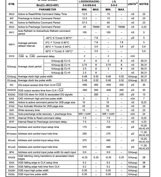
TRFC最小为105/5=21 = 0x15个时钟周期:

DDR_CONFIG_TRRD_SET(0x7) | \
TRRD最小为10/5=2 = 0x2个时钟周期

DDR_CONFIG_TRP_SET(0x9) | \
TRP最小为15/5=2 = 0x3个时钟周期

DDR_CONFIG_TRCD_SET(0x9) | \
TRCD最小为15/5=3 = 0x3个时钟周期

DDR_CONFIG_TRAS_SET(0x1b)
TRAS 最小为9个时钟周期
TRAS=max(Tras_min,tRcd+CL) = MAX(45,15+4) = 45 /5 =9

#define CFG_DDR2_CONFIG2_VAL DDR_CONFIG2_HALF_WIDTH_LOW_SET(0x1) | \
DDR_CONFIG2_SWAP_A26_A27_SET(DDR_CONFIG2_SWAP_A26_A27_VAL) \
DDR_CONFIG2_GATE_OPEN_LATENCY_SET(0x8) | \
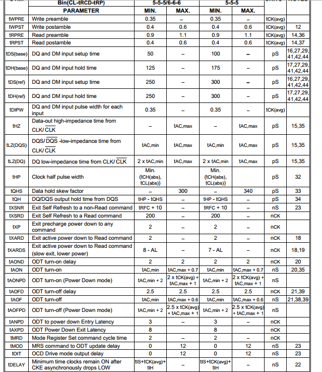
DDR_CONFIG2_TWTR_SET(0x15) | \
TWTR=[1+BL/2+tWTR/tCK]*2 = [1+8/2+ROUND_UP(7.5/5) ] *2 = [1+4+2 ] * 2 = 14 = 0xE

DDR_CONFIG2_TRTP_SET(0x9) | \
TRTP= BL/2 +max(tRTP,2)-2 = 8/2 + max(2,2) -2 = 4;

DDR_CONFIG2_TRTW_SET(0xe) | \
TRTW = (CL+BL/2) *2 = (3+8/2)*2 = 14
DDR_CONFIG2_TWR_SET(0x1) | \
TWR= [BL/2 + tWR/tCK ] * 2 -1 = [8/2 + 15/5] *2-1 = [4+3]*2-1=13 (?)

DRAM CKE bit
DDR_CONFIG2_CKE_SET(0x1) | \
Control bit to allow the memory control to tri-state the address/control outputs;
DDR_CONFIG2_CNTL_OE_EN_SET(0x1) | \
DRAM burst type Sequential;
DDR_CONFIG2_BURST_LENGTH_SET(0x8)
DRAM burst length setting,Only 8 is supported
#define CFG_DDR2_CONFIG3_VAL 0x0000000a
#define CFG_DDR2_EXT_MODE_VAL 0x402
#define CFG_DDR2_MODE_VAL_INIT 0x143
#define CFG_DDR2_MODE_VAL 0x43
#define CFG_DDR2_TAP_VAL 0x10
#define CFG_DDR2_EN_TWL_VAL 0x0000167d
#define CFG_DDR2_RD_DATA_THIS_CYCLE_VAL_16 0xffff
#define CFG_DDR2_RD_DATA_THIS_CYCLE_VAL_32 0xff

 浙公网安备 33010602011771号