The Basics of the Doherty Amplifier-Bill Slade [转载]
Introduction
The year is 1936. The boom times of the 1920s are a distant memory as the Great Depression grinds on. President Roosevelt's New Deal keeps many from starving in the streets. However, a political battle rages as congressional Republicans and the Supreme Court seek to roll back some of FDR's stimulus program, which they see as unconstitutional and unfriendly to business. The President, in turn, seeks to consolidate his power. A generation of Americans have learned the hard way how to make a dollar go a long way. “Brother can you spare a dime?” The President's “Fireside Chats” on the wireless help to bolster courage (as well as political support) among citizens as the dark clouds of war gather on the horizon.
Radio station operators were not exempt from the economic calamity that had engulfed the world. Pinching pennies was almost everyone's major activity in those days. It was in this context that William Doherty conceived his eponymous amplifier [3]. As broadcast radio and trans-oceanic radio-telephony grew in importance, powerful transmitters were needed. Amplitude modulation was the main modulation scheme, which meant that the final power amplifier had to preserve signal fidelity. Because of the characteristics of the AM signal, common Class AB amplifiers would, on average, operate very inefficiently (around 33%) because peak efficiency is obtained only by running the amplifier near its compression point1. Much of the electric power, which cost real money, did little more than heat up the surroundings. When one operated a 50kW broadcast station or a 500kW trans-atlantic shortwave transmitter, that 100kW to 1MW of waste heat produced exorbitant electric bills!
The problem is that for amplitude modulation (whether old-style double-sideband AM with carrier or without the carrier, or single-sideband), a low-distortion RF power amplifier is needed to maintain fidelity in the signal. The most efficient RF power amplifiers of the day were typically Class-C. Class-C amplifiers are non-linear (produce high distortion) and do not maintain suitable fidelity for AM signals (but work fine for constant-carrier applications like FM and on-off keying like morse code). What Mr. Doherty did was combine the Class AB and Class C amplifiers in an amazingly clever way such that overall amplifier linearity could be maintained while almost doubling the DC to RF efficiency.
Although incorporated in a number of high power broadcast stations over the years, the Doherty amplifier fell into disuse. Interest in the Doherty would be re-sparked by something Mr. Doherty could never have foreseen: the rise of digital radio communications. Complex modulation schemes like orthogonal frequency division multiplexing (OFDM) and code-division schemes like CDMA produce signals that spend most of their time around some low average but occasionally
1 Most AM transmitters of the day used a powerful audio amplifier to directly modulate the plate voltage of the final RF amplifier stage. The RF stage would actually operate near compression, but the audio amplifier driving the RF final would suffer the inefficiencies described here. Doherty's aim was to modulate the carrier further up the transmitter chain, before the final amplifier, reducing system size and permitting other forms of amplitude modulation to be used (e.g. single-sideband, frequency multiplexing for long distance telephone links, etc.)
produce signal peaks that require 6, 8, 12dB of power amplifier headroom to be held in reserve. A Class-AB amplifier can provide the needed linearity, but the overall DC to RF conversion efficiency is not at all good because the amplifier operates far from its compression point most of the time. For a cellular base station or digital TV transmitter, excessive waste heat serves no useful purpose and adds cost to the service being provided. For a hand-held, battery operated transmitting gadget, talk time is severely curtailed by inefficiency. If simultaneous optimization of amplifier linearity and efficiency are your design goals, Mr. Doherty's amplifier may provide the solution.
In this article, we will review the behavior of the Class-AB and Class-C amplifiers and then take a detailed look at how these two amplifier types can be combined to produce a system that preserves signal fidelity as well as boosts efficiency. In a 21st century interpretation of the spirit of the 1930s radio-builders, we construct a computer model of the Doherty amplifier to demonstrate how the constituent system blocks work together to produce high DC to RF conversion efficiency at “backed-off” power levels while maintaining the capacity to reproduce signal peaks high above the average signal power level.
The reader should keep in mind that this is an introductory discussion. We discuss the basics of Doherty operation, but space does not permit a full exploration of the complex details of optimizing operation of the Doherty amplifier. The interested reader is referred to the references listed at the end of this article for more rigorous presentations.
Class AB and Class C amplifiers
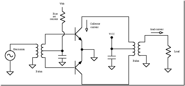
For the purpose of simulation, we will base our amplifier stages on the transformer coupled push- pull amplifier from [1] seen in Figure 1.
Figure 1: Generic push-pull stage used in Class AB and Class C amplifier simulations.
In reality, a practical implementation would look somewhat different, but the transformer coupling and the separate base and collector bias inputs provide convenient points to adjust simulation variables (e.g. bias, input and output coupling) for this simulation study of the Doherty amplifier.
Class AB amplifier
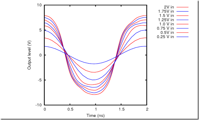
The amplifier in Figure 1 can be made to operate in Class AB by adjusting the base bias Vbb such that a small quiescent current flows in each collector (i.e. the transistors are biased at their “turn- on” point with no signal present). The amplifier will be designed to operate at 500 MHz (arbitrarily selected frequency). When sinusoidal RF excitation is applied at the input, a well reproduced sinusoidal output is produced at the output until the amplifier begins to compress. This is clearly evident from the distortion in the shapes of the higher level waveforms in Figure 2.
At low input levels (0.25 to 1V) the amplifier output level is proportional to the level of the input and the linear gain of the amplifier. We also see that the signal is nicely sinusoidal (low distortion). As the input signal level increases beyond 1V, the output level is no longer proportional to the input. The amplifier goes into compression. Moreover, the wave becomes somewhat distorted.
An important point to keep in mind is the fact that this particular Class AB amplifier appears much like a current source when operating in its low-level “linear” mode (because the transistor collectors drive the output transformer). The output impedance is relatively high, as a consequence. However, when the amplifier saturates, it begins to look more like a voltage source. The transistor collector impedance falls off because now we see the low impedance of the power- supply rails. The transistor is nearly fully “on” when saturated.
Figure 2: Output of Class AB amplifier as input levels increase.
Class C
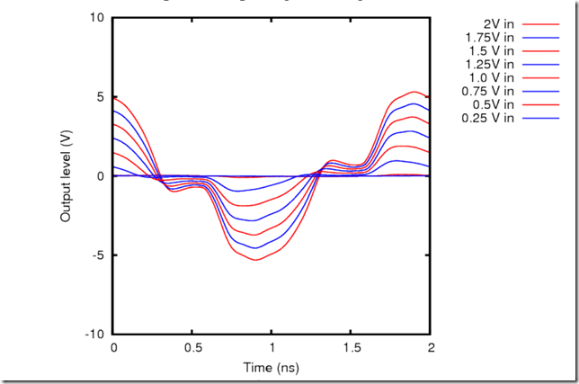
By modifying the bias point of the amplifier in Figure 1, we can make a Class-C amplifier. In this case, the transistors are biased below their cutoff point . With low-signal input, this amplifier passes negligible collector current but “wakes up” at high input signal levels. Typical Class-C behavior is observed in the amplifier output signal in Figure 3.
Notice how the output begins to appear when the input voltage is around 0.75V. The signal is very “peaky” with significant periods where the transistors are “off” (the plateaus near the 0V load voltage). Clearly, the output signal distortion shows that signal fidelity is not preserved in this amplifier under any circumstances. How do we use two distorting amplifiers to produce a final output signal with suitable fidelity?
The Doherty concept
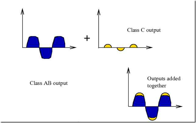
The idea is to use the Class C amplifier to “top up” the signal when the Class AB amplifier goes into compression. Below a certain point, the Class AB amplifier runs the show. We will call the Class AB stage the “carrier” amplifier. When the signal is near its average level, the Class-C stage is not operating, yet the carrier amplifier is operating near its compression point, hence operating at its most efficient level (ideally near 78%). Once peaks appear, the Class C stage starts to operate and “tops-up” the now compressing Class AB stage, pictorially presented in Figure 4. The Class C stage we will call the “peaking amplifier.”
The clever part comes in the techniques used to split the input signal suitably as well as how to combine the output signals from the carrier amplifier and the peaking amplifier such that the
Figure 3: Class C output signal for varying input signal levels.
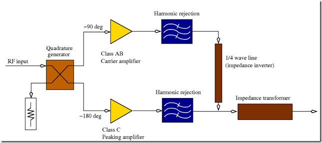
stages operate without loading each other undesirably. Put another way, we do not want the peaking amplifier to load the carrier amplifier. Likewise, once the carrier amplifier is saturated, we do not want it to load the peaking amplifier. We now come to the architecture of the Doherty amplifier (Figure 5).
Figure 4: Illustration of the Doherty idea. Above the level where the Class AB stage compresses, the Class-C stage "tops-up" the signal, restoring signal fidelity.
Figure 5: The Doherty amplifier. Note how the outputs of the constituent amplifiers are combined.
Moving from left to right in Figure 5, a quadrature hybrid produces two outputs that are 90 degrees out of phase with each other, just like in the usual “balanced” amplifier approach familiar
to microwave engineers. The 90 degree split is needed because the peaking amplifier output requires a 90 degree delay with respect to the carrier amplifier in order to be in step with the carrier amplifier output, which is subjected to a 90 degree delay in the 1⁄4 wave impedance inverter.
We then have the carrier and peaking amplifier modules that provide the gain. The output of the carrier amplifier is passed through the 1⁄4 wave line, and tied to the output of the peaking amplifier and the impedance transformer.
All the building blocks of the Doherty are now present. Now, let us examine some of the details of each of the passive building blocks before constructing the full model.
The input phasing and power split
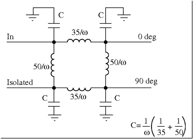
In the simulations, the power-splitting quadrature hybrid is implemented using discrete components arranged as in Figure 6.
Figure 6: Lumped component version of 3dB quadrature hybrid.
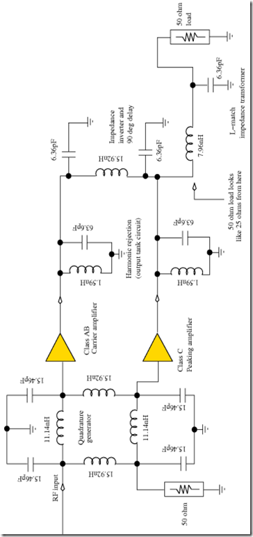
At 500 MHz (the operating frequency of our amplifier), the inductor values are 11.14nH and 15.92nH for the 35 and 50 ohm branches, respectively. The capacitor takes a value of 15.46pF
The 0 degree arm of the hybrid (shown as -90 deg in Fig. 5) is connected to the carrier amplifier and the 90 degree arm (shown as -180 in Fig. 5) goes to the peaking amplifier input. This provides the proper phasing for the clever output combining circuit to do its job.
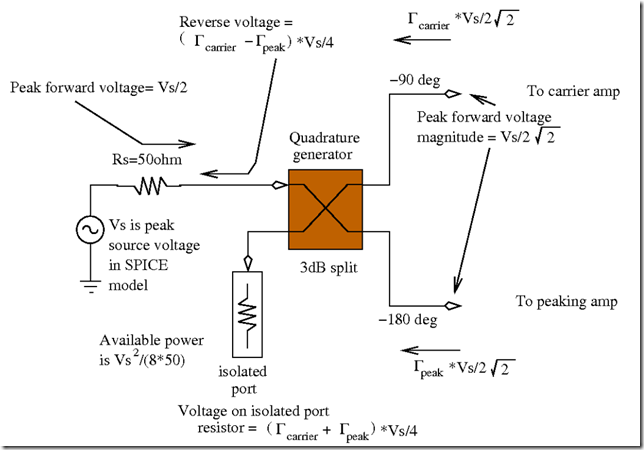
At this point, a few words are needed on the definition of input power used in the analysis of the Doherty amplifier. Since the hybrid performs a 3dB power split (half the power to the 0 (-90) arm
and half to the 90 (-180) degree arm means the voltage split is 1/2 or 0.71. The voltage sources are specified by their peak sinusoidal value Vs, so the available power before the hybrid is Vs2/2∗4∗50=Vs2/400 . One factor of 1⁄2 arises because of the time averaging of the voltage squared and the factor of 1⁄4 comes about because of the voltage divider effect of the 50 ohm source resistance. Figure 7 illustrates the effect of the hybrid on the voltages presented to the carrier and peaking amplifier inputs.
Figure 7: The properties of the power-splitting hybrid.
The reflection coefficient from the carrier amplifier is carrier and the reflection from the peaking amplifier is denoted by peak . Using a hybrid combiner in this fashion tends to assist
with input matching by routing a significant portion of any possible reflected power from the amplifiers to the isolated port resistive load instead of back into the driving source. In fact, if the reflection coefficients of the carrier and peaking amplifier are almost equal, the input source will see an almost matched load. Moreover, reflections from the one amplifier input do not affect the other amplifier because of the isolation provided by the hybrid (as long as the power source on the RF input is matched to 50 ohms). This is a common feature of all “balanced” input architectures. We can compare the reflection from a Doherty example with the input to a single Class AB stage (Figure 8).
Figure 8: Reflection coefficient versus forward input power for Class AB (blue) and the Doherty (red). Low power is on the left and the reflection coefficient moves clockwise with increasing input power level. The outer circle indicates reflection coefficient magnitude of one.
The reflection coefficient magnitude for the Class AB changes dramatically with respect to input power whereas the Doherty displays significantly less variation. Moreover, the Doherty input reflection coefficient is markedly smaller than the Class AB indicating a better input match over its full power range.
Output combining and phasing
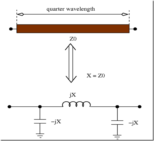
The key to combining the amplifier outputs lies in the use of an impedance inverter that ties the carrier amplifier to the output of the peaking amplifier and the impedance transformer on the output. An impedance inverter performs the function of the 1⁄4 wave transmission line. An impedance inverter will perform no impedance transformation if terminated in its characteristic impedance. Otherwise, it will transform a low impedance at one end to a high impedance at the other (and vice-versa). In our simulations, the 50 ohm transmission line in Figure 5 will be replaced with a lumped element equivalent: a pi network seen in Figure 9.
Figure 9: The 1/4 wave line can be replaced with a pi network to make an impedance inverter. The reactance of the discrete components should equal the characteristic impedance of the transmission line for proper operation.
Consistent with the “topping up” action of the peaking amplifier, when the Doherty amplifier is running with a low input drive signal, the peaking amplifier is mostly inactive and looks nearly like an open circuit. The impedance transformer converts the 50 ohm load to a 25 ohm load on the input side. In turn, the impedance inverter steps up the impedance seen by the carrier amplifier output to nearly 100 ohms. As the Doherty drive level increases, the peaking amplifier begins to conduct more and more, feeding current into the output circuit. The carrier amplifier output, because of its phase relationship of the peaking amplifier output and the 90 degree delay produced by the impedance inverter, sees its load impedance drop as input RF power increases. This “impedance modulation” effect allows the carrier amplifier output voltage to remain close to the rail voltage over a wide range of input signal levels. The load-line of the carrier amplifier changes dynamically in step with the input signal level. In other words, the peaking amplifier provides a form of fundamental active load pulling [4] to the carrier amplifier (to put this impedance modulation phenomenon in more modern terms). This is the key to the Doherty's high efficiency. Furthermore, as the carrier amplifier saturates, its output impedance drops as the transistor collectors no longer look like current sources, but voltage sources. The impedance inverter transforms the carrier amplifier output impedance to a high value, allowing the peaking amplifier transistor collectors to efficiently pump power into the load, acting as current sources. Put another way, the impedance inverter transforms the saturated carrier amplifier (now looking like a voltage source) into a current source. The peaking amplifier and carrier amplifiers behave as two parallel current sources providing power to the output network. The output circuit looks simple, but a complicated physical process is taking place.
The full model
In Figure 5, one sees band-pass filters placed after the amplifiers but before the output network. This is to reduce harmonic content that can disturb the proper functioning of the circuit. These band-pass filters are traditionally the LC output tank circuits of the carrier and peaking amplifiers. The 50 ohm load on the output is transformed to the required 25 ohms using an L-match LC network. The full model for the 500MHz Doherty amplifier is shown in Figure 10. Note that this circuit is “constructed” to highlight the operation of the individual stages for didactic purposes. A real-world amplifier would combine components, reducing component count.
Figure 10: Complete model of 500MHz Doherty amplifier showing values for passive elements.
Results
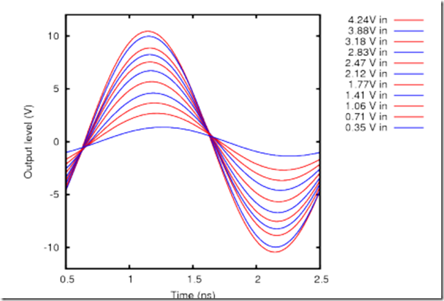
Figure 11 shows the simulated excursion of the output (load) voltage versus time for increasing source voltages in the Doherty amplifier.
If we recall the behavior of the Class AB amplifier earlier in this article, we remember that it went into compression when the source voltage exceeded 1V. Since we use a 3dB quadrature hybrid here to divide the input power and distribute it to the carrier and peaking amplifiers, a voltage of about 1.41V on the Doherty input will put the carrier amplifier into compression. It is at this point that the peaking amplifier begins topping up the output level. A small amount of distortion is apparent in the uneven signal level spacing between curves at higher drive levels. However, the waveforms look much cleaner and the compression is “softer” than that of the Class AB output shown previously. Further performance comparison can be made observing the power/efficiency plot below.
Figure 11: Output of Doherty amplifier vs. input signal level.
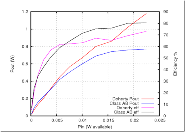
Figure 12: Power output and efficiency of carrier and full Doherty amplifier versus input power.
The blue curve shows the power output of the carrier amplifier (operating independently) as the amplifier available (forward) input power is increased. The characteristic roll-off of compression becomes apparent in the carrier amplifier as the forward input power increases above 5 mW. The red curve (the Doherty power output) continues to increase with available input power as the peaking amplifier output increases.
Of particular interest is the Doherty collector efficiency (pink curve). At an input power of 2.5 mW (output power: 200mW), the efficiency already exceeds 50% in this particular case. When the Doherty is generating 1200mW (maximum power shown here), the carrier amplifier can no longer be said to operate in class AB, but more like Class D (transistors are “fully on” or “fully off”). This is why the carrier amplifier efficiency (the black curve) exceeds the Class AB theoretical limit of 78%. The carrier amplifier would be clipping strongly if operating independently of the peaking amplifier.
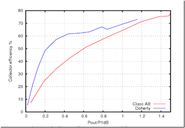
Making similar headroom available in a Class AB amplifier would mean the amplifier would spend most of its time operating with an efficiency of about 10-15%. This fact is reinforced by observing the difference in efficiency versus normalized output power in Figure 13. Use of a Class AB amplifier would not be acceptable from an power efficiency perspective and would require excessive over-engineering of the amplifier just to accommodate the headroom needed for peak power requirements.
Figure 13: Behavior of collector efficiency versus amplifier output power (normalized to P1dB level). Note how the Doherty amplifier operates at high efficiency well before overall compression starts.
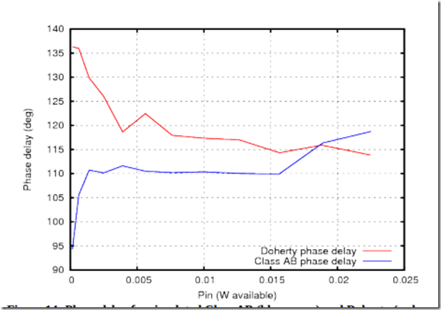
Amplitude compression is important, but represents only part of the complex behavior of power amplifiers. The Class AB and the Doherty will also exhibit phase distortion as a function of power. This is the so-called AM-PM (amplitude modulation to phase modulation) distortion. Figure 14 shows the variation of amplifier phase delay for the Class AB and Doherty amplifiers.
Figure 14: Phase delay for simulated Class AB (blue curve) and Doherty (red curve) amplifiers.
The phase delay for the Class AB experiences a sudden shift when the input signal power rises above the small signal level (1-2mW) and remains flat, even when the amplifier goes into compression. The Doherty results, on the other hand, exhibit a more gradual shift at low powers, but then level off above 5mW input power.
Phase distortion is important to consider because many modern modulation schemes require good phase fidelity to maximize data transport capability of the communication channel. The phase performance will be highly dependent on the implementation and a full description is beyond the scope of this introductory article. The reader is referred to in-depth articles (e.g. [5]) for techniques to correct amplifier phase errors.
Conclusions
The Doherty amplifier is an ideal candidate for maximizing the power amplifier efficiency while simultaneously maintaining amplifier linearity (faithful signal reproduction) for signals with high peak-to-average power ratios. If the modulation scheme is based on some form of frequency division multiplexing or amplitude modulation, the Doherty amplifier is a possible candidate topology. If your application calls for a constant carrier modulation scheme (FM, FSK, PSK, etc.), then the Doherty is not suitable. In this case a Class C or one of the switching amplifier topologies may be appropriate. To sum up some of the pros and cons of the Doherty:
Pros:
- Good way to stretch amplifier efficiency while achieving good signal fidelity
- Reduces spectral regrowth in signals with high peak to average power ratios when compared to Class AB operating near compression point
- Can be used in low-power (handheld) as well as high power (e.g. broadcast) amplifiers.
Lots of ways to optimize for various applications (bias, phasing).
- Balanced input circuit reduces return loss variation and magnitude over power range. Cons:
- Increased circuit complexity over classical Class AB amplifier topology.
- Difficult to tune all parameters to find best operating point (operating sweet spot).
- Device parasitics complicate design of real-world amplifier.
- Input signal levels change operating characteristics (this is true for other large-signal amplifier types as well).
- Doherty amplifier gain is lower (often approximately 3dB lower) than for corresponding Class AB amplifier because of power-splitting at input needed for carrier and peaking amplifiers.
- References
- Class AB and C amplifiers [1] B. Slade, “Amplifier Alphabet Soup: Part I, Basics of Class A, AB, B and C amplifiers,” RF Globalnet, Feb. 2011. Simulation All simulations in this article were carried out using NGSpice [2] models. The reader is referred to the following websites for more information on these packages. [2] http://ngspice.sourceforge.net/ General reading The reader is who wishes a more in-depth treatment of the subject of RF and microwave power amplifiers can consult some of the works used in the preparation of this article.
. [3] W. H. Doherty, “A new high-efficiency power amplifier for modulated waves,” Bell Telephone Laboratories monograph B-931, May 1936. (available online at http://sujan.hallikainen.org/BroadcastHistory/uploads/Doherty.pdf)
. [4] S. C. Cripps, RF Power Amplifiers for Wireless Communications, Artech House, 1999.
. [5] M. Elmala, J. Paramesh and K. Soumyanath, “A 90-nm CMOS Doherty power amplifier with minimum AM-PM distortion,” IEEE Trans. Solid State Circ., vol. 41, no. 6, June 2006.




 浙公网安备 33010602011771号