
[SILVACO ATLAS]a-IGZO薄膜晶体管二维器件仿真(01)
最近因为肺炎的缘故,宅在家里不能出门,就翻了下一些资料,刚好研究方向是这个,就简单研究了下。参考资料主要如下:
1.《半导体工艺和器件仿真软件Silvaco TCAD实用教程》 唐龙谷 2014
2.《长安大学 半导体工艺与器件仿真指导书》 张林 2015
引用本科时社团一姐的一句话:学习PS的精髓在于毁图。个人浅见,学习仿真的话还是要根据实例拆解分析比较快。重复,我是新手,只是个人浅见。
官网实例:https://www.silvaco.com/examples/tcad/section41/index.html
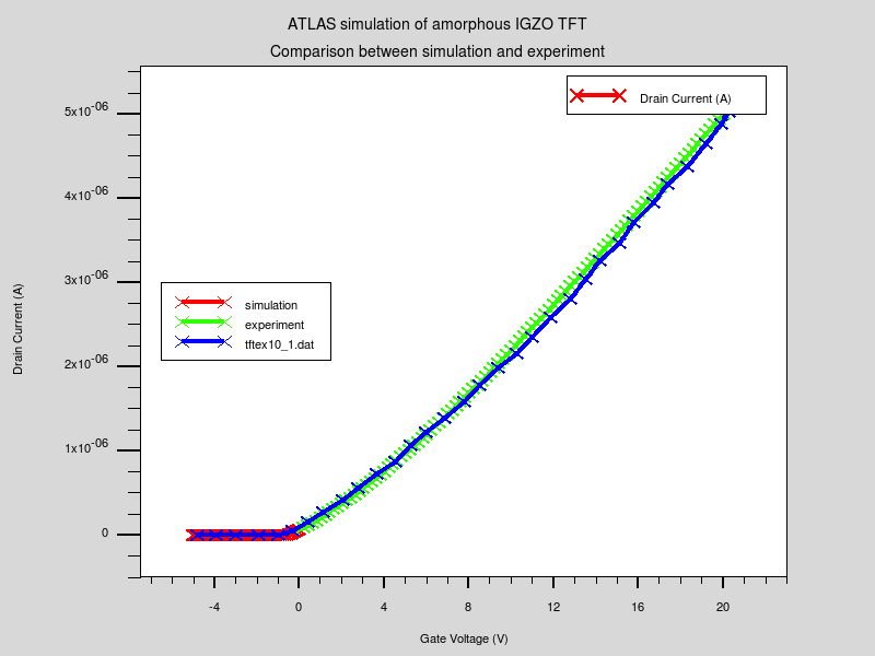
tftex10.in : Amorphous IGZO TFT Simulation:

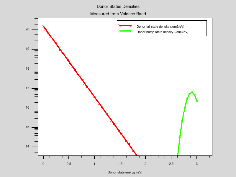
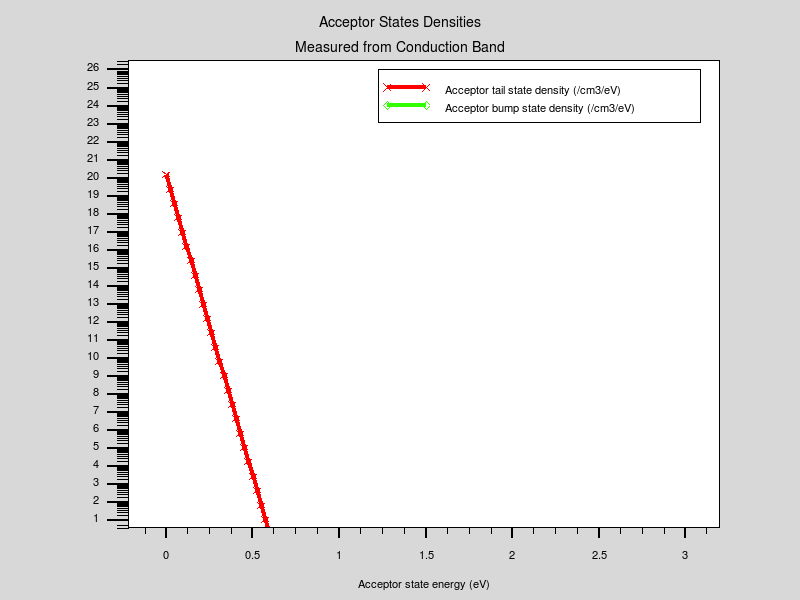
# (c) Silvaco Inc., 2019 # This example demonstrates simulation of amorphous IGZO (indium galium # zinc oxide) TFT. Here we reproduce the results from: # # Fung, T., Chuang, C., Chen, C., Katsumi, A., Cottle, R., Townsend, M., # Kumomi, H., and Kanicki, J., "Two-dimensional numerical simulation of # radio frequency sputter amorphous In-Ga-Zn-O thin-film transistors", # J. Appl. Phys., V. 106, pp. 084511-1 through 084511-10. # # Comparisons with experiment are included. # # This first part of the input deck simulates Id-Vg. # go atlas mesh width=180 outf=tftex10_1.str master.out x.m l=0 s=0.25 x.m l=40 s=0.25 y.m l=0 s=0.0005 y.m l=0.02 s=0.0005 y.m l=0.12 s=0.005 #(划分网格) # The device is composed of a 20 nm layer of IGZO deposited # 100 nm oxide on a n++ substrate that acts as the gate. # region num=1 material=igzo y.min=0 y.max=0.02 region num=2 material=sio2 y.min=0.02 y.max=0.12 #(定义材料) elec num=1 name=gate bottom elec num=2 name=source y.max=0.0 x.min=0.0 x.max=5.0 elec num=3 name=drain y.max=0.0 x.min=35.0 x.max=40.0 #(定义电极) # We define the gate as N.POLY. This pins the gate workfunction # to the conduction band edge of silicon. # contact num=1 n.poly # # We also define a workfunction for the source and drain that # is very close to the conduction edge. In the reference the # authors observed that without a workfunction the results for # ohmic boundaries were not significantly different than the # Schottky model. # contact num=2 workf=4.33 contact num=3 workf=4.33 #(定义接触条件) models fermi # # Key to the characterization of amorphous materials is the # definition of the states within the band gap. # defects nta=1.55e20 ntd=1.55e20 wta=0.013 wtd=0.12 \ nga=0.0 ngd=6.5e16 egd=2.9 wgd=0.1 \ sigtae=1e-15 sigtah=1e-15 sigtde=1e-15 sigtdh=1e-15 \ siggae=1e-15 siggah=1e-15 siggde=1e-15 siggdh=1e-15 \ dfile=tftex10_don.dat afile=tftex10_acc.dat numa=128 numd=64 #(定义缺陷分布) # From here we simply extract the Id-Vg characteristic # solve init solve prev
#??? solve vdrain=0.1 save outf=tftex10_0.str log outf=tftex10_1a.log solve vgate=0 vstep=-0.1 vfinal=-5 name=gate log off
#??? load inf=tftex10_0.str master solve prev log outf=tftex10_1b.log solve vstep=0.2 vfinal=20.0 name=gate # # And we compare the simulation with experimental data reported in # the reference. # tonyplot -overlay tftex10_1a.log tftex10_1b.log tftex10_1.dat -set tftex10_1.set #tonyplot 的 overlay与set命令 ??? tonyplot -overlay tftex10_don.dat -set tftex10_don.set
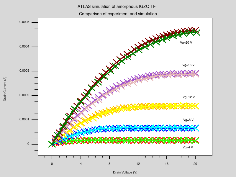
#绘制施主态密度分布曲线 tonyplot -overlay tftex10_acc.dat -set tftex10_acc.set #绘制受主态密度分布曲线 go atlas # # In the next part of the input deck we extract the Id-Vd family of # curves. The structure definition is exactly the same. # mesh width=180 x.m l=0 s=0.25 x.m l=40 s=0.25 y.m l=0 s=0.0005 y.m l=0.02 s=0.0005 y.m l=0.12 s=0.005 region num=1 material=igzo y.min=0 y.max=0.02 region num=2 material=sio2 y.min=0.02 y.max=0.12 elec num=1 name=gate bottom elec num=2 name=source y.max=0.0 x.min=0.0 x.max=5.0 elec num=3 name=drain y.max=0.0 x.min=35.0 x.max=40.0 contact num=1 n.poly contact num=2 workf=4.33 contact num=3 workf=4.33 models fermi defects nta=1.55e20 ntd=1.55e20 wta=0.013 wtd=0.12 \ nga=0.0 ngd=6.5e16 egd=2.9 wgd=0.1 \ sigtae=1e-15 sigtah=1e-15 sigtde=1e-15 sigtdh=1e-15 \ siggae=1e-15 siggah=1e-15 siggde=1e-15 siggdh=1e-15 \ dfile=don afile=acc numa=128 numd=64 # # Here we calculate the start structures for each of the IdVd # family by performing an initial gate ramp. #
#(下面就有点懵了...)
solve solve vstep=0.2 vfinal=4.0 name=gate save outf=tftex10_2.str
solve vstep=0.2 vfinal=8.0 name=gate save outf=tftex10_3.str
solve vstep=0.2 vfinal=12.0 name=gate save outf=tftex10_4.str
solve vstep=0.2 vfinal=16.0 name=gate save outf=tftex10_5.str
solve vstep=0.2 vfinal=20.0 name=gate save outf=tftex10_6.str

load inf=tftex10_2.str master log outf=tftex10_2.log
solve vdrain=0.0 vstep=0.5 vfinal=20.0 name=drain

load inf=tftex10_3.str master log outf=tftex10_3.log
solve vdrain=0.0 vstep=0.5 vfinal=20.0 name=drain

load inf=tftex10_4.str master log outf=tftex10_4.log
solve vdrain=0.0 vstep=0.5 vfinal=20.0 name=drain

load inf=tftex10_5.str master log outf=tftex10_5.log
solve vdrain=0.0 vstep=0.5 vfinal=20.0 name=drain

load inf=tftex10_6.str master log outf=tftex10_6.log
solve vdrain=0.0 vstep=0.5 vfinal=20.0 name=drain

tonyplot -overlay tftex10_2.log tftex10_2.dat tftex10_3.log tftex10_3.dat tftex10_4.log tftex10_4.dat tftex10_5.log tftex10_5.dat tftex10_6.log tftex10_6.dat -set tftex10_2.set

quit
官网给出的四张输出图像如下:
自己装的ATLAS还有点问题,这几天先折腾下在跑跑看。
不过毕竟是引用了别人的文献中的数据,与实验室的材料特性还有较大差距,估计要手调了。
总体来说,ATLAS的步骤主要为:
建立网格-定义材料-定义电极以及接触-定义缺陷分布或掺杂-引入模型以及求解方法-求解-Tonyplot输出
要解决的难点主要在于:
1.材料特性微调;
2.缺陷分布调整;
3.理解输出语句,并合理运用;
武汉加油!
【推荐】编程新体验,更懂你的AI,立即体验豆包MarsCode编程助手
【推荐】凌霞软件回馈社区,博客园 & 1Panel & Halo 联合会员上线
【推荐】抖音旗下AI助手豆包,你的智能百科全书,全免费不限次数
【推荐】博客园社区专享云产品让利特惠,阿里云新客6.5折上折
【推荐】轻量又高性能的 SSH 工具 IShell:AI 加持,快人一步