u-boot移植(七)---代码修改---存储控制器
一、CPU访问芯片的条件

CPU通过访问存储控制器,来读取外部设备的数据。
CPU想访问一个芯片,需要如下条件(配置信息):
-
- 地址线
- 数据线:8位/16位/32位数据宽度
- 时钟/频率
- 其他芯片相关的特性:比如SDRAM,有行地址、列地址和bank
SDRAM的访问和表格检索的原理一样,先指定一个行(Row),再指定一个列(Columu),就可以准确找到所需要的单元格。这个单元格称为存储单元,这个表格(存储阵列)就是逻辑Bank(Logical Bank,即L-Bank),SDRAM一般含有4个L-bank。

只有配置好了存储管理器,才知道如何去访问外部的设备。
二、存储控制器访问SDRAM
2.1 原理图

CPU侧:


可以看看这些引脚的功能,查看SDRAM的芯片手册。
LADDR:地址接口

LnWBE[0:3]:bank的操作方式

LDATA:数据接口

LnWE

更多的看数据手册。
三、存储管理器的配置
- 位宽
- 行列地址
- 刷新周期
详细寄存器可以查看DATASHEET。
四、2440启动方式
4.1 NAND FALSH启动

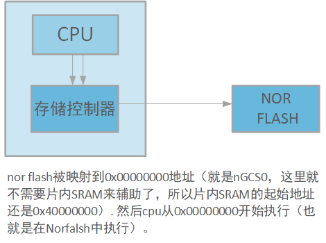
4.2 NOR FLASH
五、代码
内存控制器初始化代码:
这里我们是从nor flash启动,因此CONFIG_SYS_TEXT_BASE定义的参数为0x0。
lowlevel_init.S (board\samsung\jz2440)
  1 #define BWSCON    0x48000000
  2
  3 /* BWSCON */
  4 #define DW8            (0x0)
  5 #define DW16            (0x1)
  6 #define DW32            (0x2)
  7 #define WAIT            (0x1<<2)
  8 #define UBLB            (0x1<<3)
  9
 10 #define B1_BWSCON        (DW32)
 11 #define B2_BWSCON        (DW16)
 12 #define B3_BWSCON        (DW16 + WAIT + UBLB)
 13 #define B4_BWSCON        (DW16)
 14 #define B5_BWSCON        (DW16)
 15 #define B6_BWSCON        (DW32)
 16 #define B7_BWSCON        (DW32)
 17
 18 /* BANK0CON */
 19 #define B0_Tacs            0x0    /*  0clk */
 20 #define B0_Tcos            0x0    /*  0clk */
 21 #define B0_Tacc            0x7    /* 14clk */
 22 #define B0_Tcoh            0x0    /*  0clk */
 23 #define B0_Tah            0x0    /*  0clk */
 24 #define B0_Tacp            0x0
 25 #define B0_PMC            0x0    /* normal */
 26
 27 /* BANK1CON */
 28 #define B1_Tacs            0x0    /*  0clk */
 29 #define B1_Tcos            0x0    /*  0clk */
 30 #define B1_Tacc            0x7    /* 14clk */
 31 #define B1_Tcoh            0x0    /*  0clk */
 32 #define B1_Tah            0x0    /*  0clk */
 33 #define B1_Tacp            0x0
 34 #define B1_PMC            0x0
 35
 36 #define B2_Tacs            0x0
 37 #define B2_Tcos            0x0
 38 #define B2_Tacc            0x7
 39 #define B2_Tcoh            0x0
 40 #define B2_Tah            0x0
 41 #define B2_Tacp            0x0
 42 #define B2_PMC            0x0
 43
 44 #define B3_Tacs            0x0    /*  0clk */
 45 #define B3_Tcos            0x3    /*  4clk */
 46 #define B3_Tacc            0x7    /* 14clk */
 47 #define B3_Tcoh            0x1    /*  1clk */
 48 #define B3_Tah            0x0    /*  0clk */
 49 #define B3_Tacp            0x3     /*  6clk */
 50 #define B3_PMC            0x0    /* normal */
 51
 52 #define B4_Tacs            0x0    /*  0clk */
 53 #define B4_Tcos            0x0    /*  0clk */
 54 #define B4_Tacc            0x7    /* 14clk */
 55 #define B4_Tcoh            0x0    /*  0clk */
 56 #define B4_Tah            0x0    /*  0clk */
 57 #define B4_Tacp            0x0
 58 #define B4_PMC            0x0    /* normal */
 59
 60 #define B5_Tacs            0x0    /*  0clk */
 61 #define B5_Tcos            0x0    /*  0clk */
 62 #define B5_Tacc            0x7    /* 14clk */
 63 #define B5_Tcoh            0x0    /*  0clk */
 64 #define B5_Tah            0x0    /*  0clk */
 65 #define B5_Tacp            0x0
 66 #define B5_PMC            0x0    /* normal */
 67
 68 #define B6_MT            0x3    /* SDRAM */
 69 #define B6_Trcd            0x1
 70 #define B6_SCAN            0x1    /* 9bit */
 71
 72 #define B7_MT            0x3    /* SDRAM */
 73 #define B7_Trcd            0x1    /* 3clk */
 74 #define B7_SCAN            0x1    /* 9bit */
 75
 76 /* REFRESH parameter */
 77 #define REFEN            0x1    /* Refresh enable */
 78 #define TREFMD            0x0    /* CBR(CAS before RAS)/Auto refresh */
 79 #define Trp            0x0    /* 2clk */
 80 #define Trc            0x3    /* 7clk */
 81 #define Tchr            0x2    /* 3clk */
 82 #define REFCNT            1113    /* period=15.6us, HCLK=60Mhz, (2048+1-15.6*60) */
 83 /**************************************/
 84
 85 .globl lowlevel_init
 86 lowlevel_init:
 87     /* memory control configuration */
 88     /* make r0 relative the current location so that it */
 89     /* reads SMRDATA out of FLASH rather than memory ! */
 90     /* 初始化内存 */
 91     ldr     r0, =SMRDATA            /* 将SMRDATA的首地址(第一个.long)内存单元数据放置到r0寄存器中 r0=eac */
 92     ldr    r1, =CONFIG_SYS_TEXT_BASE    /* CONFIG_SYS_TEXT_BASE=0x0(include/configs/jz2440中定义)
 93                                        代码的基地址 */
 94     sub    r0, r0, r1                    /* r0 = r0 -r1 */
 95     ldr    r1, =BWSCON    /* Bus Width Status Controller,BWSCON=0x48000000,此文件中定义 */
 96     add     r2, r0, #13*4            /* 将SMRDATA这一块地址赋值给r2中 */
 97 0:
 98     ldr     r3, [r0], #4            /* 将r0的值代表的内存单元放入r3中,之后r0的值偏移4位 */
 99     str     r3, [r1], #4            /* 将r3的值放入r1的值代表的地址中,r1的值代表的地址偏移4位 */
100     cmp     r2, r0                    /* 比较r2 和 r0 ,若不相等则执行下一句*/
101     bne     0b                        /* 向后跳转到标签0处*/
102
103     /* everything is fine now */
104     mov    pc, lr                        /* 返回 */
105
106     .ltorg
107 /* the literal pools origin */
108
109 /*
110  * 初始化存储控制器,经过此初始化之后,内存才可以使用
111  */
112  /* 地址为 0x00000eb0 */
113 SMRDATA:
114         .long 0x22011110     //BWSCON
115         .long 0x00000700     //BANKCON0
116         .long 0x00000700     //BANKCON1
117         .long 0x00000700     //BANKCON2
118         .long 0x00000700     //BANKCON3
119         .long 0x00000740     //BANKCON4
120         .long 0x00000700     //BANKCON5
121         .long 0x00018005     //BANKCON6
122         .long 0x00018005     //BANKCON7
123         .long 0x008C04F4     //REFRESH
124         .long 0x000000B1     //BANKSIZE
125         .long 0x00000030     //MRSRB6
126         .long 0x00000030     //MRSRB7

 浙公网安备 33010602011771号