

谈谈FPGA设计的实现过程-设计流程入门01
00
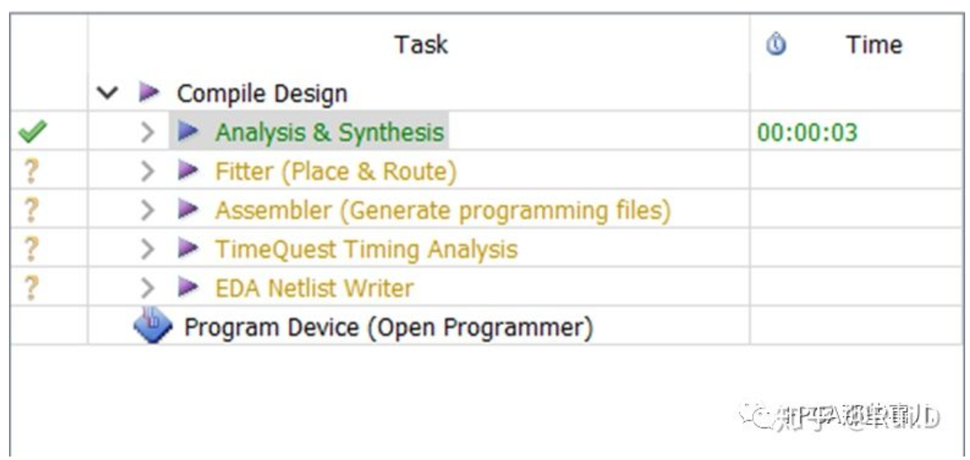
概括来说,FPGA的实现过程分为2步:分析综合与布局布线。这一点,在Quartus II软件中体现的尤为明显。

这是Quartus II软件在编译时的任务栏。红框中的两步,正是分析综合与布局布线。
而在Altera中,将编译与映射合称为综合。
因此这样看来,整个实现过程,其实包含编译、映射、布局、布线这4个步骤。
为了更好地解释,我们以一段代码为例进行说明。
01

module led_test
(
  input           clk,        //时钟
  input           rst_n,      //复位
  input           a,
  input           b,
  input           c,
  input           d,
  output reg      led,
  output reg      led_2
);

always@(posedge clk or negedge rst_n)
begin
  if (rst_n == 1'b0)
    led <= 0;
  else
    led <= (a&&b)||(c||d);
end

always@(negedge clk or negedge rst_n)
begin
  if (rst_n == 1'b0)
    led_2 <= 0;
  else
    led_2 <= (a||b)&&(c&&d);
end

endmodule
非常简单的一段代码,主要构建了两个寄存器,实现了两组4输入的逻辑关系。在Quartus II中双击“Analysis&Synthesis”,完成分析与综合,如上所述,点击一次,其实是完成了编译、映射两步。
02
所谓的编译实现了什么?编译将原理图、HDL代码、IP软核生成了门级网表。门级网表中,描述的电路元件基本是门,或与此同级别的元件。
说的再通俗些,就是将我们的代码,变成了由与门、或门、非门、触发器、加法器、多路选择器等等构成的数字电路。
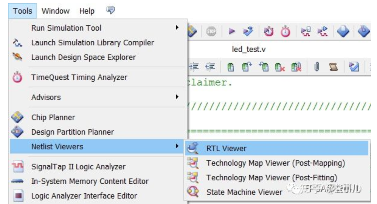
在Quartus II中,点击“RTL Viewer”这一项,就能看到我们编译后生成的门级网表。
本例中的代码,生成了这样的门级电路。很显然,此图功能与Verilog代码一致。
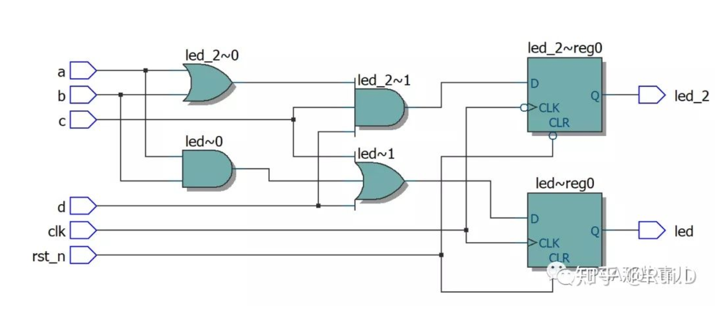
总结一下,编译将原理图、HDL代码、IP软核生成了门级网表。而且这个门级网表其实与所用的器件无关。无论是Cyclone IV还是Stratix V,上面的代码都会被编译为这样的原理图。
另外需要说明的是,Quartus II可以对编译施加一些约束,比如使门级网表“速度优先”还是“面积优先”。这样一来,相同的代码经过不同的约束,有可能生成不同的网表,但不管怎说,编译都是一个与器件型号无关的过程。
03
接下来讲讲映射(Mapping)。我们知道,实际上FPGA中并没有与门、或门、非门等门电路,这些逻辑关系,都是由查找表LUT所实现的。所以很自然我们得到,编译过后,下一步的内容,就是把编译得到的网表,转换为LUT实现,而这正是映射的目的。
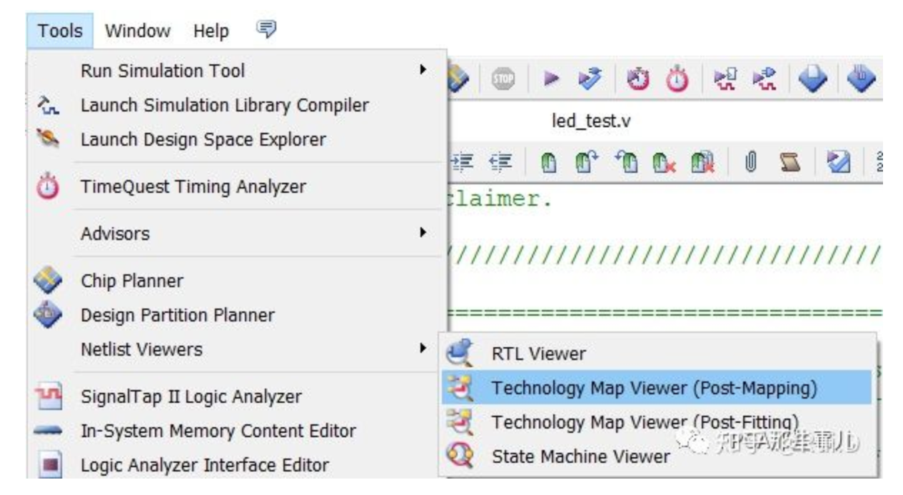
与上一步类似,点击“Technology Map Viewer(Post-Mapping)”这一项,就能看到我们映射后的LUT实现。
上图中的门级网表,转换成了这样的LUT实现。
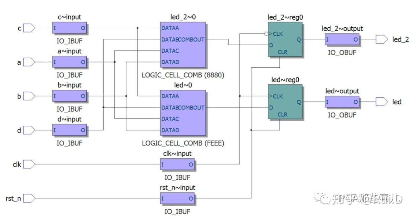
其中,2个LOGIC_CELL_COMB就是2个LUT,而8880与FEEE,则是LUT中的16进制数值。
显然,映射是一个与器件有关的过程。因为不同型号的FPGA有不同的LUT,比如Cyclone IV与Cyclone V的LUT结构就不同,这一点我们以后再聊。
说完了映射,其实就说完了综合。关于综合的作用,其实从另一个地方也能看到一些端倪。双击“Analysis&Synthesis”之后,工程目录下的output文件夹下会出现一个名为"工程名.map.rpt"的文件,这个文件Quartus II在映射之后给出的报告。用记事本打开,里面含有以下内容。
+---------------------------------------------+---------+
; Estimated Total logic elements              ; 2       ;
;                                             ;         ;
; Total combinational functions               ; 2       ;
; Logic element usage by number of LUT inputs ;         ;
;     -- 4 input functions                    ; 2       ;
;     -- 3 input functions                    ; 0       ;
;     -- <=2 input functions                  ; 0       ;
;                                             ;         ;
; Logic elements by mode                      ;         ;
;     -- normal mode                          ; 2       ;
;     -- arithmetic mode                      ; 0       ;
;                                             ;         ;
; Total registers                             ; 2       ;
;     -- Dedicated logic registers            ; 2       ;
;     -- I/O registers                        ; 0       ;
;                                             ;         ;
; I/O pins                                    ; 8       ;
; Embedded Multiplier 9-bit elements          ; 0       ;
; Maximum fan-out node                        ; c~input ;
; Maximum fan-out                             ; 2       ;
; Total fan-out                               ; 24      ;
; Average fan-out                             ; 1.20    ;
+---------------------------------------------+---------+
可以发现,经过映射之后,已经生成了LUT。文件中还有一些其他的配置信息,大家有兴趣的话,可以自己找到后学习研究。
04
映射之后,得到了具体的LUT网表。那么这个网表究竟该放到FPGA中的哪个部分?LUT网表与FPGA真实的结构有什么匹配关系?解决这个问题的,正是布局与布线。
点击Quanrtus II中的"Fitter(Place & Route)",完成布局布线。
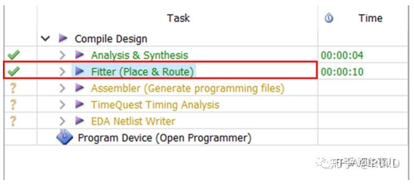
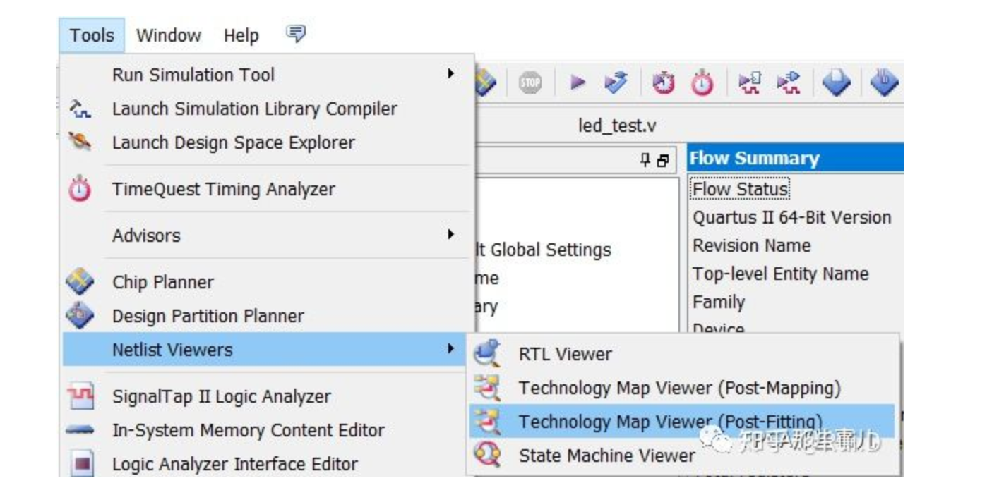
与上面的分析类似,我们点击"Technology Map Viewer(Post-Fitting)"来看看布局布线后生成的电路图。
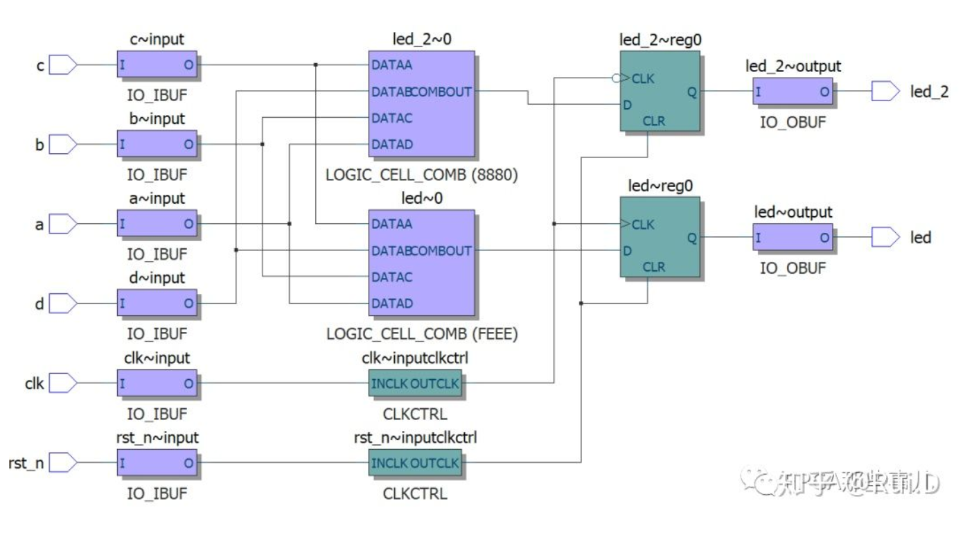
Technology Map Viewer(Post-Fitting)后的图
与上面“Technology Map Viewer(Post-Mapping)”后的图相比,主要差别在于,多了两个绿色的"CLKCTRL"模块,这两个模块说明,clk与rst_n这两个信号,被分配到了全局时钟信号。关于全局时钟信号,我们会在之后的文章中讲解。总的来说,这说明映射之后的LUT图被Quartus II匹配到了FPGA芯片中特定的位置,同时完成了各个模块之间的走线。
与上文类方法类似,在Fitter(Place & Route)之后,工程下面的output文件夹下生成一个名为"工程名.fit.rpt"的文件,这个文件报告了在布局布线之后的信息,用记事本打开,里面含有以下内容。这些是具体输入输出引脚,在FPGA芯片中的具体位置及相关属性。
+----------------------------------------------------------------------------------------------------------------------------------------------------------------------------------------------------------------------------------------------------------------------------+
; Input Pins                                                                                                                                                                                                                                                                 ;
+-------+-------+----------+--------------+--------------+--------------+-----------------------+--------------------+--------+----------------+---------------+-----------------+----------+--------------+--------------+---------------------------+----------------------+
; Name  ; Pin # ; I/O Bank ; X coordinate ; Y coordinate ; Z coordinate ; Combinational Fan-Out ; Registered Fan-Out ; Global ; Input Register ; Power Up High ; PCI I/O Enabled ; Bus Hold ; Weak Pull Up ; I/O Standard ; Termination Control Block ; Location assigned by ;
+-------+-------+----------+--------------+--------------+--------------+-----------------------+--------------------+--------+----------------+---------------+-----------------+----------+--------------+--------------+---------------------------+----------------------+
; a     ; Y6    ; 3        ; 5            ; 0            ; 14           ; 2                     ; 0                  ; no     ; no             ; no            ; yes             ; no       ; Off          ; 3.3-V LVTTL  ; --                        ; Fitter               ;
; b     ; AA4   ; 3        ; 7            ; 0            ; 0            ; 2                     ; 0                  ; no     ; no             ; no            ; yes             ; no       ; Off          ; 3.3-V LVTTL  ; --                        ; Fitter               ;
; c     ; AB3   ; 3        ; 5            ; 0            ; 0            ; 2                     ; 0                  ; no     ; no             ; no            ; yes             ; no       ; Off          ; 3.3-V LVTTL  ; --                        ; Fitter               ;
; clk   ; G1    ; 1        ; 0            ; 30           ; 7            ; 2                     ; 0                  ; yes    ; no             ; no            ; yes             ; no       ; Off          ; 3.3-V LVTTL  ; --                        ; Fitter               ;
; d     ; AA3   ; 3        ; 5            ; 0            ; 7            ; 2                     ; 0                  ; no     ; no             ; no            ; yes             ; no       ; Off          ; 3.3-V LVTTL  ; --                        ; Fitter               ;
; rst_n ; T2    ; 2        ; 0            ; 30           ; 14           ; 2                     ; 0                  ; yes    ; no             ; no            ; yes             ; no       ; Off          ; 3.3-V LVTTL  ; --                        ; Fitter               ;
+-------+-------+----------+--------------+--------------+--------------+-----------------------+--------------------+--------+----------------+---------------+-----------------+----------+--------------+--------------+---------------------------+----------------------+


+----------------------------------------------------------------------------------------------------------------------------------------------------------------------------------------------------------------------------------------------------------------------------------------------------------------------------------------------------------------------------------------------------------------------------------+
; Output Pins                                                                                                                                                                                                                                                                                                                                                                                                                      ;
+-------+-------+----------+--------------+--------------+--------------+-----------------+------------------------+---------------+-----------+-----------------+------------+---------------+----------+--------------+--------------+------------------+-------------+---------------------------+----------------------------+-----------------------------+----------------------+----------------------+---------------------+
; Name  ; Pin # ; I/O Bank ; X coordinate ; Y coordinate ; Z coordinate ; Output Register ; Output Enable Register ; Power Up High ; Slew Rate ; PCI I/O Enabled ; Open Drain ; TRI Primitive ; Bus Hold ; Weak Pull Up ; I/O Standard ; Current Strength ; Termination ; Termination Control Block ; Output Buffer Pre-emphasis ; Voltage Output Differential ; Location assigned by ; Output Enable Source ; Output Enable Group ;
+-------+-------+----------+--------------+--------------+--------------+-----------------+------------------------+---------------+-----------+-----------------+------------+---------------+----------+--------------+--------------+------------------+-------------+---------------------------+----------------------------+-----------------------------+----------------------+----------------------+---------------------+
; led   ; Y4    ; 3        ; 3            ; 0            ; 7            ; no              ; no                     ; no            ; 2         ; no              ; no         ; no            ; no       ; Off          ; 3.3-V LVTTL  ; 8mA              ; Off         ; --                        ; no                         ; no                          ; Fitter               ; -                    ; -                   ;
; led_2 ; Y3    ; 3        ; 3            ; 0            ; 0            ; no              ; no                     ; no            ; 2         ; no              ; no         ; no            ; no       ; Off          ; 3.3-V LVTTL  ; 8mA              ; Off         ; --                        ; no                         ; no                          ; Fitter               ; -                    ; -                   ;
+-------+-------+----------+--------------+--------------+--------------+-----------------+------------------------+---------------+-----------+-----------------+------------+---------------+----------+--------------+--------------+------------------+-------------+---------------------------+----------------------------+-----------------------------+----------------------+----------------------+---------------------+05
05
至此,我们讲完了编译、映射、布局、布线这四个步骤的具体作用,这里总结一下。
编译:将原理图、HDL代码、IP软核生成门级网表。
映射:把编译得到的网表,转换为FPGA中的LUT实现。
布局:将已连接好的LUT合理地放到特定的FPGA中。
布线:将现有的模块连接起来,本质上是一个线路分布求最优的问题。
OK,这次我们就说这么多,下次再见!
欢迎大家关注我的微信公众号:FPGA里的那些事儿,一起学习与闲聊。


【推荐】国内首个AI IDE,深度理解中文开发场景,立即下载体验Trae
【推荐】编程新体验,更懂你的AI,立即体验豆包MarsCode编程助手
【推荐】抖音旗下AI助手豆包,你的智能百科全书,全免费不限次数
【推荐】轻量又高性能的 SSH 工具 IShell:AI 加持,快人一步
· TypeScript + Deepseek 打造卜卦网站:技术与玄学的结合
· 阿里巴巴 QwQ-32B真的超越了 DeepSeek R-1吗?
· 【译】Visual Studio 中新的强大生产力特性
· 10年+ .NET Coder 心语 ── 封装的思维:从隐藏、稳定开始理解其本质意义
· 【设计模式】告别冗长if-else语句:使用策略模式优化代码结构