

DMA数据存储进度获取
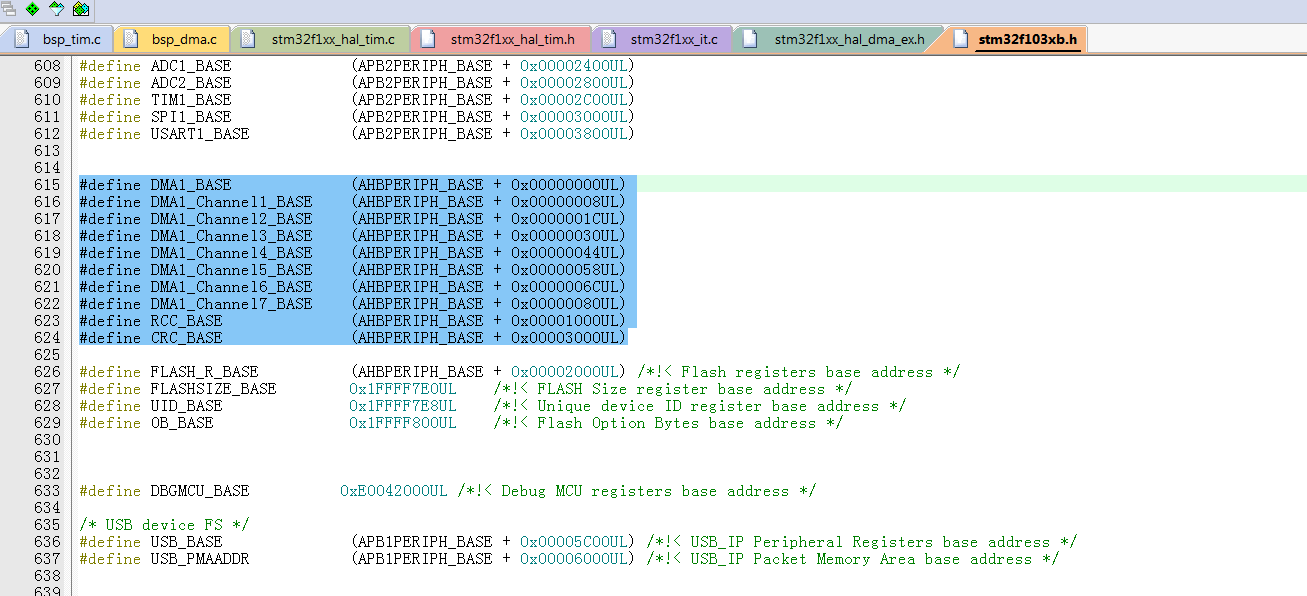
1 2 3 4 5 6 7 8 9 10 | #define DMA1_BASE (AHBPERIPH_BASE + 0x00000000UL)#define DMA1_Channel1_BASE (AHBPERIPH_BASE + 0x00000008UL)#define DMA1_Channel2_BASE (AHBPERIPH_BASE + 0x0000001CUL)#define DMA1_Channel3_BASE (AHBPERIPH_BASE + 0x00000030UL)#define DMA1_Channel4_BASE (AHBPERIPH_BASE + 0x00000044UL)#define DMA1_Channel5_BASE (AHBPERIPH_BASE + 0x00000058UL)#define DMA1_Channel6_BASE (AHBPERIPH_BASE + 0x0000006CUL)#define DMA1_Channel7_BASE (AHBPERIPH_BASE + 0x00000080UL)#define RCC_BASE (AHBPERIPH_BASE + 0x00001000UL)#define CRC_BASE (AHBPERIPH_BASE + 0x00003000UL)<br><br> |
int16_t p=0;//剩余RAM空间
p=*(volatile uint16_t*)(DMA1_Channel5_BASE+0x0C + 20 x (5 – 1)); //DMA1_Channel5_CNDTR5
或者
p=DMA1_Channel5->CNDTR;
https://blog.csdn.net/qq_40544107/article/details/105186669
1 2 3 4 5 6 7 8 9 10 11 12 13 14 15 16 17 18 19 20 21 22 23 24 25 26 27 28 29 30 31 32 33 34 35 36 37 38 39 40 41 42 43 44 45 | /** @addtogroup Peripheral_declaration * @{ */ #define TIM2 ((TIM_TypeDef *)TIM2_BASE)#define TIM3 ((TIM_TypeDef *)TIM3_BASE)#define TIM4 ((TIM_TypeDef *)TIM4_BASE)#define RTC ((RTC_TypeDef *)RTC_BASE)#define WWDG ((WWDG_TypeDef *)WWDG_BASE)#define IWDG ((IWDG_TypeDef *)IWDG_BASE)#define SPI2 ((SPI_TypeDef *)SPI2_BASE)#define USART2 ((USART_TypeDef *)USART2_BASE)#define USART3 ((USART_TypeDef *)USART3_BASE)#define I2C1 ((I2C_TypeDef *)I2C1_BASE)#define I2C2 ((I2C_TypeDef *)I2C2_BASE)#define USB ((USB_TypeDef *)USB_BASE)#define CAN1 ((CAN_TypeDef *)CAN1_BASE)#define BKP ((BKP_TypeDef *)BKP_BASE)#define PWR ((PWR_TypeDef *)PWR_BASE)#define AFIO ((AFIO_TypeDef *)AFIO_BASE)#define EXTI ((EXTI_TypeDef *)EXTI_BASE)#define GPIOA ((GPIO_TypeDef *)GPIOA_BASE)#define GPIOB ((GPIO_TypeDef *)GPIOB_BASE)#define GPIOC ((GPIO_TypeDef *)GPIOC_BASE)#define GPIOD ((GPIO_TypeDef *)GPIOD_BASE)#define GPIOE ((GPIO_TypeDef *)GPIOE_BASE)#define ADC1 ((ADC_TypeDef *)ADC1_BASE)#define ADC2 ((ADC_TypeDef *)ADC2_BASE)#define ADC12_COMMON ((ADC_Common_TypeDef *)ADC1_BASE)#define TIM1 ((TIM_TypeDef *)TIM1_BASE)#define SPI1 ((SPI_TypeDef *)SPI1_BASE)#define USART1 ((USART_TypeDef *)USART1_BASE)#define DMA1 ((DMA_TypeDef *)DMA1_BASE)#define DMA1_Channel1 ((DMA_Channel_TypeDef *)DMA1_Channel1_BASE)#define DMA1_Channel2 ((DMA_Channel_TypeDef *)DMA1_Channel2_BASE)#define DMA1_Channel3 ((DMA_Channel_TypeDef *)DMA1_Channel3_BASE)#define DMA1_Channel4 ((DMA_Channel_TypeDef *)DMA1_Channel4_BASE)#define DMA1_Channel5 ((DMA_Channel_TypeDef *)DMA1_Channel5_BASE)#define DMA1_Channel6 ((DMA_Channel_TypeDef *)DMA1_Channel6_BASE)#define DMA1_Channel7 ((DMA_Channel_TypeDef *)DMA1_Channel7_BASE)#define RCC ((RCC_TypeDef *)RCC_BASE)#define CRC ((CRC_TypeDef *)CRC_BASE)#define FLASH ((FLASH_TypeDef *)FLASH_R_BASE)#define OB ((OB_TypeDef *)OB_BASE)#define DBGMCU ((DBGMCU_TypeDef *)DBGMCU_BASE) |
typedef struct
{
  __IO uint32_t CCR;
  __IO uint32_t CNDTR;
  __IO uint32_t CPAR;
  __IO uint32_t CMAR;
} DMA_Channel_TypeDef;

/* Memory mapping of Core Hardware */
#define SCS_BASE (0xE000E000UL) /*!< System Control Space Base Address */
#define ITM_BASE (0xE0000000UL) /*!< ITM Base Address */
#define DWT_BASE (0xE0001000UL) /*!< DWT Base Address */
#define TPI_BASE (0xE0040000UL) /*!< TPI Base Address */
#define CoreDebug_BASE (0xE000EDF0UL) /*!< Core Debug Base Address */
#define SysTick_BASE (SCS_BASE + 0x0010UL) /*!< SysTick Base Address */
#define NVIC_BASE (SCS_BASE + 0x0100UL) /*!< NVIC Base Address */
#define SCB_BASE (SCS_BASE + 0x0D00UL) /*!< System Control Block Base Address */

#define SCnSCB ((SCnSCB_Type *) SCS_BASE ) /*!< System control Register not in SCB */
#define SCB ((SCB_Type *) SCB_BASE ) /*!< SCB configuration struct */
#define SysTick ((SysTick_Type *) SysTick_BASE ) /*!< SysTick configuration struct */
#define NVIC ((NVIC_Type *) NVIC_BASE ) /*!< NVIC configuration struct */
#define ITM ((ITM_Type *) ITM_BASE ) /*!< ITM configuration struct */
#define DWT ((DWT_Type *) DWT_BASE ) /*!< DWT configuration struct */
#define TPI ((TPI_Type *) TPI_BASE ) /*!< TPI configuration struct */
#define CoreDebug ((CoreDebug_Type *) CoreDebug_BASE) /*!< Core Debug configuration struct */

【推荐】国内首个AI IDE,深度理解中文开发场景,立即下载体验Trae
【推荐】编程新体验,更懂你的AI,立即体验豆包MarsCode编程助手
【推荐】抖音旗下AI助手豆包,你的智能百科全书,全免费不限次数
【推荐】轻量又高性能的 SSH 工具 IShell:AI 加持,快人一步
· TypeScript + Deepseek 打造卜卦网站:技术与玄学的结合
· 阿里巴巴 QwQ-32B真的超越了 DeepSeek R-1吗?
· 【译】Visual Studio 中新的强大生产力特性
· 10年+ .NET Coder 心语 ── 封装的思维:从隐藏、稳定开始理解其本质意义
· 【设计模式】告别冗长if-else语句:使用策略模式优化代码结构