做详细布线(DR)前需要了解的基础概念 EDA
Component is a basic functional element of a circuit. Examples include transistors, resistors, and capacitors.
Module is a circuit partition or a grouped collection of components.
Block is a module with a shape, i.e., a circuit partition with fixed dimensions. (standard or macro cells)
Cell is a logical or functional unit built from various components. In digital circuits, cells commonly refer to gates, e.g., INV, AND-OR-INVERTER (AOI), NAND, NOR. In general, the term is used to refer to either standard cells or macros.
Pin is an electrical terminal used to connect a given component to its external environment. At the level of block-to-block connections (internal to the IC), I/O pins are present on lower-level metal layers such as Metal1, Metal2 and Metal3.
layer is a manufacturing process level in which design components are patterned. During physical design, circuit components are assigned to different layers, e.g., transistors are assigned to poly and active layers, while interconnects are assigned to poly and metal layers and are routed according to the netlist.
Via is a connection between metal layers, usually to connect routing structures on different layers.
Net or Signal is a set of pins or terminals that must be connected to have the same potential.
A typical p-pin net connects one output pin of a gate and p – 1 input pins of other gates; its fanout is equal to p – 1.
Netlist is the collection of all signal nets and the components that they connect in a design, or, a list of all the nets and connecting pins of a subsection of the design.

GR: During global routing, pins with the same electric potential are connected using wire segments.
Global routing seeks to
-
determine whether a given placement is routable.
-
determine a coarse routing for all nets within available routing regions.
Specifically, given a placement and a netlist, determine the necessary wiring, e.g., net topologies and specific routing segments, to connect these cells while respecting constraints, e.g., design rules and routing resource capacities, and optimizing routing objectives, e.g., minimizing total wirelength and maximizing timing slack.
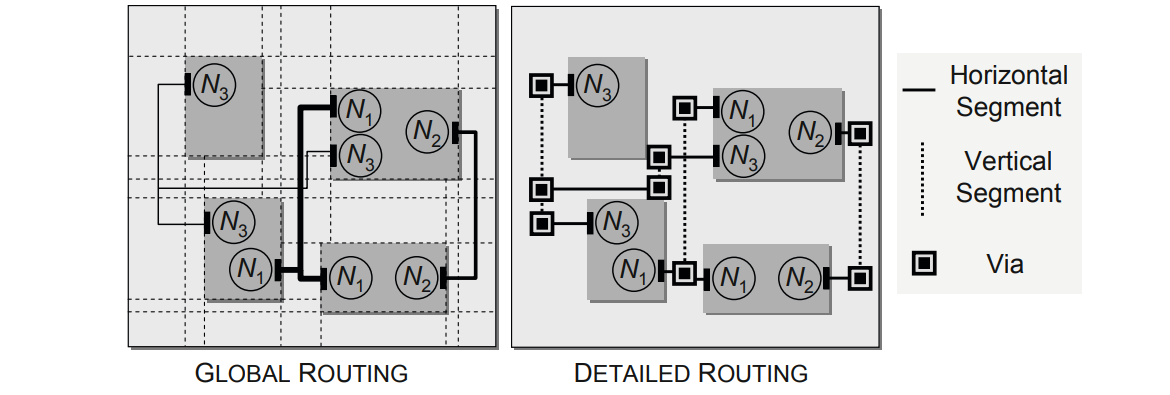
Graphical representation of nets N1-N3 that are (coarsely) globally routed using routing regions (left), and then (finely) detailed routed using rectilinear paths (right). This example assumes two-layer routing, with horizontal and vertical segments routed on separate layers.
During global routing, the wire segments used by net topologies are tentatively assigned (embedded) within the chip layout. The chip area is represented by a coarse routing grid, and available routing resources are represented by edges with capacities in a grid graph. Nets are then assigned to these routing resources.
After global routing, each net undergoes detailed routing. During detailed routing, the wire segments are assigned to specific routing tracks. This process involves a number of intermediate tasks and decisions such as net ordering, i.e., which nets should be routed first, and pin ordering, i.e., within a net, in what order should the pins be connected.
These two issues are the major challenges in sequential routing, where nets are routed one at a time. The net and pin orderings can have dramatic impacts on final solution quality. To determine the net ordering, each net is given a numerical indicator of importance (priority), known as a net weight. High priority can be given to nets that are timing-critical, connect to numerous pins, or carry specific functions such as delivering clock signals. High-priority nets should avoid unnecessary detours, even at the cost of detouring other nets. Pin ordering is typically performed using either tree-based algorithms or geometric criteria based on pin locations.
Routing Track (column) is an available horizontal (vertical) wiring path. A signal net often uses a sequence of alternating horizontal tracks and vertical columns, where adjacent tracks and columns are connected by inter-layer vias.
Routing Region is a region that contains routing tracks and/or columns.
Uniform Routing Region is formed by evenly spaced horizontal and vertical grid lines that induce a uniform grid over the chip area. This grid is sometimes referred to as a ggrid (global grid); it is composed of unit gcells (global cells). Grid lines are typically spaced 7 to 40 routing tracks apart to balance the complexities of the chip-scale global routing and gcell-scale detailed routing problems.
Non-uniform Routing Region is formed by horizontal and vertical boundaries that are aligned to external pin connections or macro-cell boundaries. This results in channels and switchboxes – routing regions that have differing sizes. During global routing, nets are assigned to these routing regions. During detailed routing, the nets within each routing region are assigned to specific wiring paths.
Channel is a rectangular routing region with pins on two opposite (usually the longer) sides and no pins on the other (usually the shorter) sides. There are two types of channels – horizontal and vertical. Horizontal channel is a channel with pins on the top and bottom boundaries. Vertical channel is a channel with pins on the left and right boundaries.
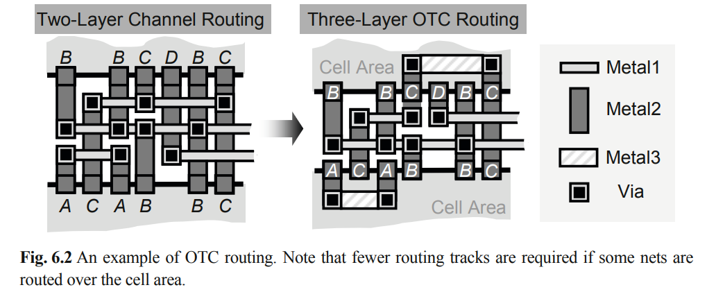
The pins of a net are connected to the routing channel by columns, which in turn are connected to other columns by tracks. In older, variable-die routing contexts, such as two-layer standard-cell routing, the channel height is flexible, i.e., its capacity can be adjusted to accommodate the necessary amount of wiring. However, due to the increased number of routing layers in modern designs, this traditional channel model has largely lost its relevance. Instead, over-the-cell (OTC) routing is used.
Channel capacity represents the number of available routing tracks or columns. For single-layer routing, the capacity is the height h of the channel divided by the pitch dpitch, where dpitch is the minimum distance between two wiring paths in the relevant (vertical or horizontal) direction. For multilayer routing, the capacity σ(Layers) is the sum of the capacities of all layers.

Here, Layers is the set of all layers, and dpitch(layer) is the routing pitch for layer.
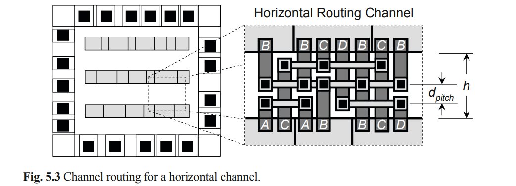
Switchbox is the intersection of horizontal and vertical channels. Due to fixed dimensions, switchbox routing exhibits less flexibility and is more difficult than channel routing. Note that since the entry points of wires are fixed, the problem is one of finding routes inside the switchbox.

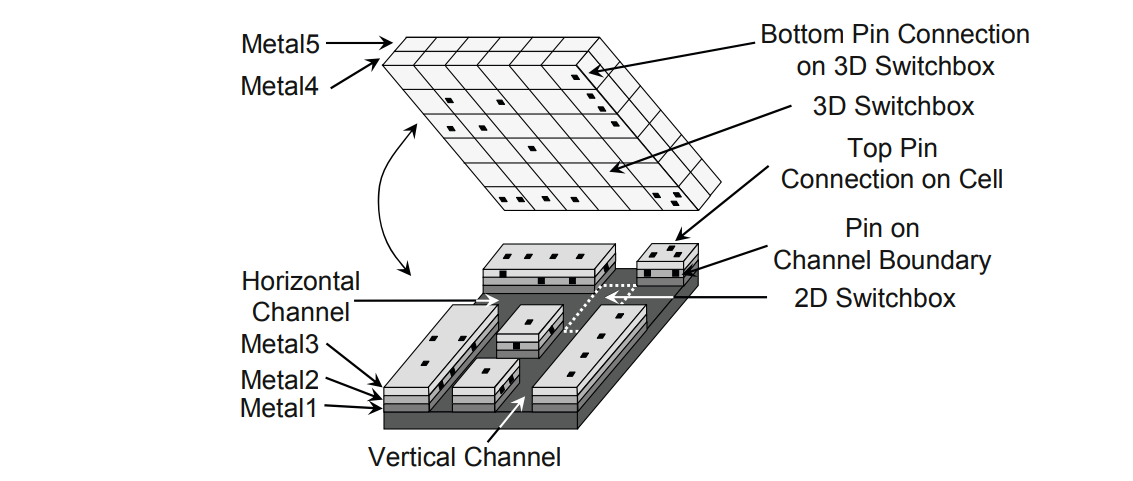
2D and 3D switchboxes in a five-layer process. The cells are internally routed using layers up to Metal3. 2D switchboxes typically exist on layers Metal1, Metal2 and Metal3. Layers Metal4 and Metal5 are connected by a 3D switchbox.
T-junction occurs when a vertical channel meets a horizontal channel.
The objective of detailed routing is to assign route segments of signal nets to specific routing tracks, vias, and metal layers in a manner consistent with given global routes of those nets. These route assignments must respect all design rules.
Each gcell is orders of magnitude smaller than the entire chip, e.g., 10 x 10 routing tracks, regardless of the actual chip size. !!! As long as the routes remain properly connected across all neighboring gcells, the detailed routing of one gcell can be performed independently of the routing of other gcells !!!
Traditional detailed routing techniques are applied within routing regions, such as channels and switchboxes. For modern designs, over-the-cell (OTC) routing allows wires to be routed over standard cells. Due to technology scaling, modern detailed routers must account for manufacturing rules and the impact of manufacturing faults. (e.g., 天线效应 PAE Process Antenna Effect 制造时蚀刻和离子注入 裸露的金属线和多晶硅收集游离电荷 从而击穿CMOS栅极,造成永久性损伤。布线过程中,连接天线二极管或跳转到上一层金属 以增强CMOS栅极静态电荷承受能力 从而预防PAE。)

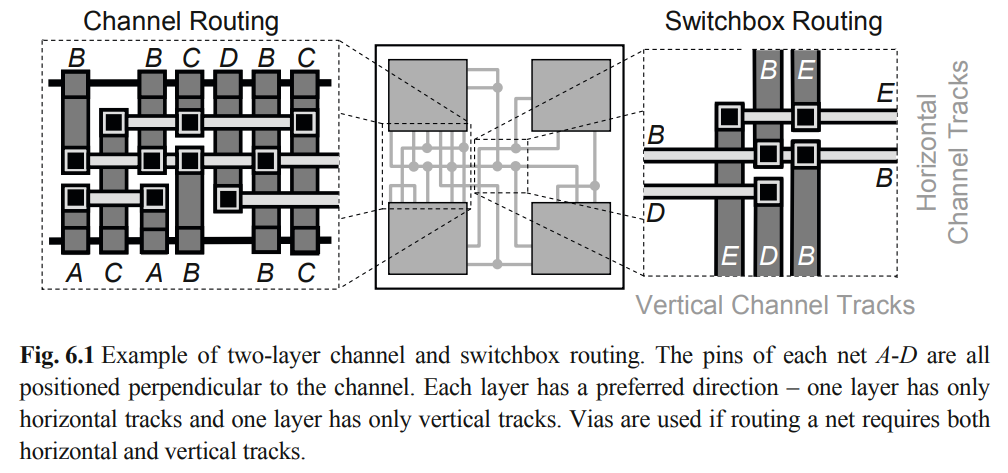
Channel routing is a special case of detailed routing where the connections between terminal pins are routed within a routing region (channel) that has no obstacles.
Switchbox routing is performed when pin locations are given on all four sides of a fixed-size routing region.
OTC (over-the-cell) routing uses additional metal tracks, e.g., on Metal3 and Metal4, that are not obstructed by cells, allowing routes to cross cells and channels. OTC routing can use only the metal layers and tracks that the cells do not occupy. When the cells utilize only the polysilicon and Metal1 layers, routing can be performed on the remaining metal layers (Metal2, Metal3, etc.) as well as unused Metal1 resources.
In classical channel routing, the routing area is a rectangular grid (Fig. 6.3) with pin locations on top and bottom boundaries. The pins are located on the vertical grid lines or columns. The channel height depends on the number of tracks that are needed to route all the nets. In two-layer routing, one layer is reserved exclusively for horizontal tracks while the other is reserved for vertical tracks. The preferred direction of each routing layer is determined by the floorplan and the orientation of the standard-cell rows. In a horizontal cell row, polysilicon (transistor gate) segments are typically vertical (V) and Metal1 segments are horizontal (H). The metal layers’ preferred directions then alternate between H and V. To connect to a cell pin that is on the Metal1 layer, the router will drop one or more vias from a Metal2 routing segment.
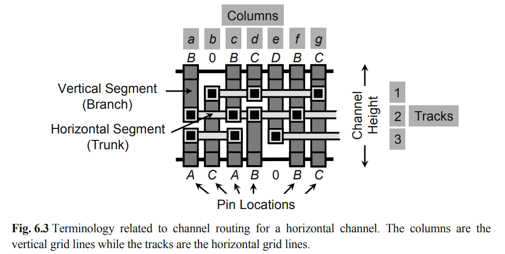
Given a channel, its upper and lower boundaries are each defined by a vector of net IDs, denoted as TOP and BOT, respectively. Here, each column is represented by two net IDs (Fig. 6.3), one from the top channel boundary and one from the bottom channel boundary. Unconnected pins are given a net ID of 0. In the example of Fig. 6.3, TOP = [B 0 B C D B C] and BOT = [A C A B 0 B C].
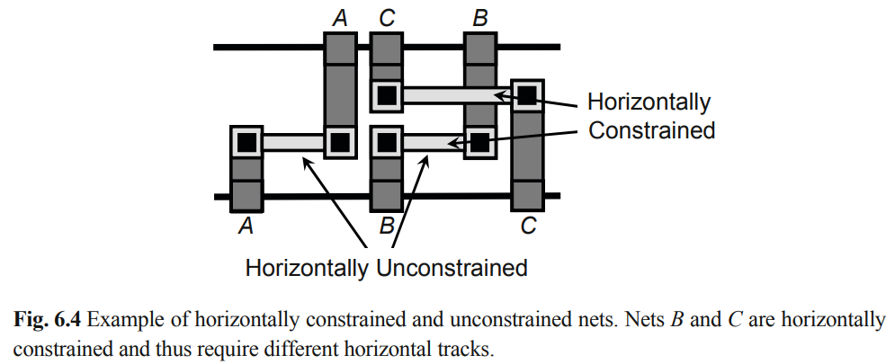
Horizontal constraint exists between two nets if their horizontal segments overlap when placed on the same track.
Vertical constraint exists between two nets if they have pins in the same column.
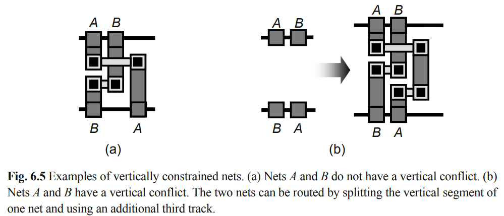
Although a vertical constraint implies a horizontal constraint, the converse is not necessarily true. However, both types of constraints must be satisfied when assigning segments in a channel.


