Graphics Data RAMs and HBM
GDRAMs or GSDRAMs (Graphics or Graphics Synchronous DRAMs) are a special class of DRAMs based on SDRAM designs but tailored for handling the higher bandwidth demands of graphics processing units. GDDR5 is based on DDR3 with earlier GDDRs based on DDR2. Because graphics processor units (GPUs; see Chapter 4) require more bandwidth per DRAM chip than CPUs, GDDRs have several important differences:
- GDDRs have wider interfaces: 32-bits versus 4, 8, or 16 in current designs.
- GDDRs have a higher maximum clock rate on the data pins. To allow a higher transfer rate without incurring signaling problems, GDRAMS normally connect directly to the GPU and are attached by soldering them to the board, unlike DRAMs, which are normally arranged in an expandable array of DIMMs.
Altogether, these characteristics let GDDRs run at two to five times the bandwidth per DRAM versus DDR3 DRAMs.
The newest innovation in 2017 in DRAMs is a packaging innovation, rather than a circuit innovation. It places multiple DRAMs in a stacked or adjacent fashion embedded within the same package as the processor. (Embedded DRAM also is used to refer to designs that place DRAM on the processor chip.) Placing the DRAM and processor in the same package lowers access latency (by shortening the delay between the DRAMs and the processor) and potentially increases band-width by allowing more and faster connections between the processor and DRAM; thus several producers have called it high bandwidth memory (HBM).
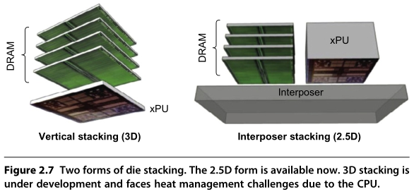
One version of this technology places the DRAM die directly on the CPU die using solder bump technology to connect them. Assuming adequate heat management, multiple DRAM dies can be stacked in this fashion. Another approach stacks only DRAMs and abuts them with the CPU in a single package using a substrate (interposer) containing the connections. Figure 2.7 shows these two different inter-connection schemes. Prototypes of HBM that allow stacking of up to eight chips have been demonstrated. With special versions of SDRAMs, such a package could contain 8 GiB of memory and have data transfer rates of 1 TB/s. The 2.5D technique is currently available. Because the chips must be specifically manufactured to stack, it is quite likely that most early uses will be in high-end server chipsets.
In some applications, it may be possible to internally package enough DRAM to satisfy the needs of the application. For example, a version of an Nvidia GPU used as a node in a special-purpose cluster design is being developed using HBM, and it is likely that HBM will become a successor to GDDR5 for higher-end applications. In some cases, it may be possible to use HBM as main memory, although the cost limitations and heat removal issues currently rule out this technology for some embedded applications. In the next section, we consider the possibility of using HBM as an additional level of cache.
Computer Architecture, Sixth Edition A Quantitative Approach by John L. Hennessy, David A. Patterson (z-lib.org)

 浙公网安备 33010602011771号