SPI总线介绍
SPI Overview


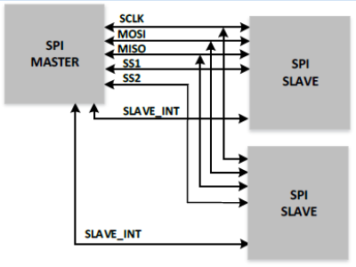
System Architecture:
- Single-master
- Multi-slave
- Serial bus.
Address space:
- no limitation
Operation modes:
- 60 Mbpsmax at 60MHz for conventional implementations
(Typical: 10 Mbps at 10 MHz)
SPI Protocol

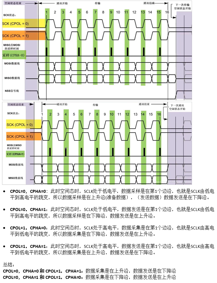
如何记忆:
cpol:IDLE state of SCK; 就是说在ilde状态下,cpol为0,则sck为低;cpol为1,则sck为高。它表示sck的极性。
cpha:对应着数据采样(即采样mosi)是在第几个边沿,0对应着第一个边沿,1对应着第二个边沿。
也就是说,cpha=0,对应在第一个边沿采样(这意味着在第一个边沿之前数据就已经ready),第二个边沿输出数据。
cpha = 1,对应在第二个边沿采样,第一个边沿输出数据。
SPI Timing
Ref:https://www.ti.com.cn/content/dam/videos/external-videos/en-us/8/3816841626001/6246789954001.mp4/subassets/adcs-spi-communications-timing-presentation.pdf
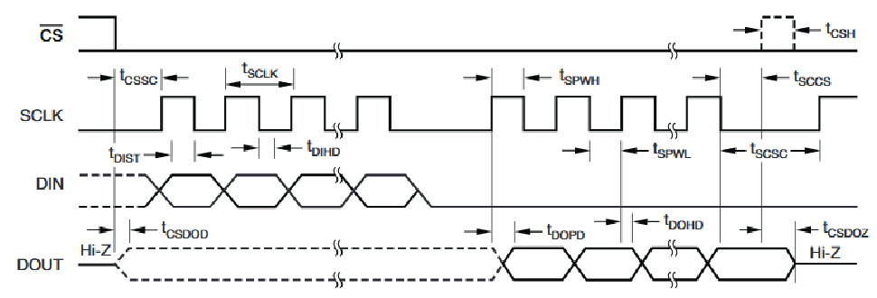
以cpol=0,cpha=1为例:

- t_CSH:Minimum pulse duration, CS high. This time defines the time required for the CS to stay high to ensure that the device has reset the SPI communications.
- t_CSSC(lead time): CS low to first SCLK high. As chip select is taken low, it still takes a small amount of time for the device to determine that it is the active peripheral.
This also allows for time to setup data that the device needs to send out on DOUT at the first SCLK rising edge pulse. A violation may cause the device to miss the first SCLK pulse. - t_SCLK: The sclk period. SCLKs can be sent to a device only so fast before the device fails to recognize it. This defines the minimum time for SCLK.
- t_SPWH, t_SPWL: The minimum time for an SCLK high and the minimum time for an SCLK low. These two times with tSCLK define how much skew in the SCLK duty cycle is allowed.
For this device, there is a maximum tSPWL for SPI timeout. - t_SCCS(lag time): Time from the falling edge of SCLK to the rising edge of CS. Because CS disables the SPI, ensure that the device receives the last bit of data before shutting down SPI communication. It is a hold time for the data with SCLK and a setup time for the chip select to the device's internal clock.
- t_DIST(MOSI setup time): the setup time for the DIN data. For data to be read into the device, the mosi must first be established for a time period before the SCLK falling edge.
- t_DIHD(MOSI hold time): the hold time for the DIN data. Once the data is set onto the mosi line, the SCLK falling edge latches the data into the device.
- t_CSDOD(MISO active time): Propagation delay time from CS falling to DOUT actively driven. When CS is high, the DOUT is high impedance(Hi-Z), allowing for multiple devices on the bus to drive DOUT a device at a time. t_CSDOD shows the propagation delay from the chip select going low to when the DOUT is active.
- t_DOPD(MISO delay): the maximum propagation delay time from the rising edge of SCLK to the data appearing on DOUT. SCLK is used to clock out data from the device. When SCLK is driven high, this signals to the device that data should be put on DOUT that can be clocked out on the falling edge of DOUT.
- t_CSDOZ(MISO tristate): Propagation delay time from rising edge of CS to DOUT becoming Hi-Z
总结:
关于sck的timing:sck period, sck high, sck low
关于CS的timing:minimum cs high
cs和sck:lead time,lag time
mosi和sck:si setup time,si hold time
miso和sck:so maximum propagation delay time
miso和cs:active time(from cs falling to so active),tristate time(from cs rising to so high-Z)
SPI IO mode
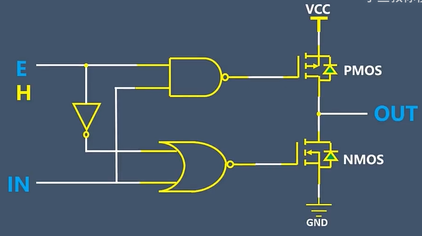
SPI IO一般设计为推挽结构,其优点是输出直接上拉到了电源,可以输出很高的电流,驱动能力强。
SPI是单Master协议,因此在mosi线上不存在“线与”的情况(一输出多)
但是miso线上存在“线与”的情况(多输出一)PS:如果只有一个SPI从设备,可以不用考虑,但是如果存在多个SPI从设备,则salver的miso需要有高阻态:
High-Z:E=0时,OUT悬空


 浙公网安备 33010602011771号