物理设计 (Physical design)
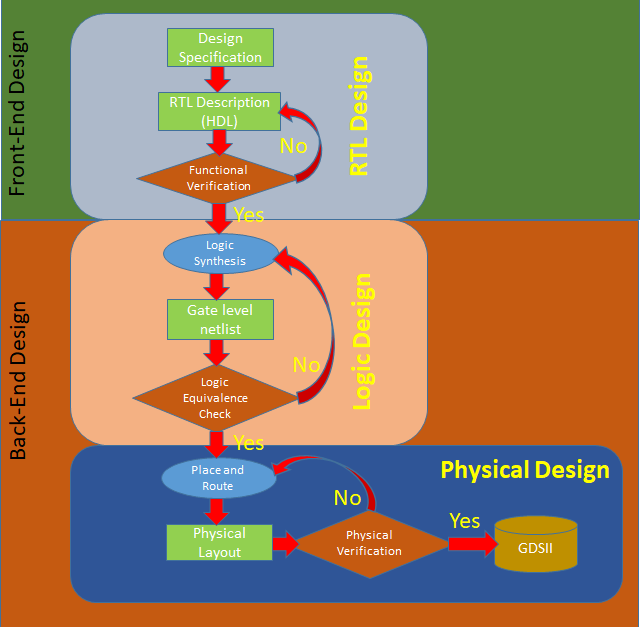
ASIC设计全流程:

ASIC Back-end Flow
Ref:IC入门必备!数字IC中后端设计实现全流程解析(1.3万字长文)

Physical Design:
Physical design: convert netlist (.v ) into GDSII form(layout form)
During physical design, all macros, cells, gates, transistors, etc., with fixed shapes and sizes per fabrication layer, are assigned spatial locations (placement) and have appropriate routing connections (routing) completed in metal layers.
The main steps in the ASIC physical design flow are:
- Design Netlist (after synthesis)
- Floorplanning
- Partitioning
- Placement
- Clock-tree Synthesis (CTS)
- Routing
- Physical Verification
Steps:
Partitioning
Partitioning is a process of dividing the chip into small blocks. This is done mainly to separate different functional blocks and also to make placement and routing easier.
This kind of partitioning is commonly referred to as Logical Partitioning. The goal of partitioning is to split the circuit such that the number of connections between partitions is minimized.
Floorplanning
Floorplanning is the process of identifying structures that should be placed close together, and allocating space for them in such a manner as to meet the sometimes conflicting goals of available space (cost of the chip), required performance, and the desire to have everything close to everything else.
Placement
Before the start of placement optimization all Wire Load Models (WLM) are removed. Placement uses RC values from Virtual Route (VR) to calculate timing.
VR is the shortest Manhattan distance between two pins. VR RCs are more accurate than WLM RCs.
Placement is performed in four optimization phases:
- Pre-placement optimization
- In placement optimization
- Post Placement Optimization (PPO) before clock tree synthesis (CTS)
- PPO after CTS.
- Pre-placement Optimization optimizes the netlist before placement, HFNs (High Fanout Nets) are collapsed. It can also downsize the cells.
- In-placement optimization re-optimizes the logic based on VR. This can perform cell sizing, cell moving, cell bypassing, net splitting, gate duplication, buffer insertion, area recovery. Optimization performs iteration of setup fixing, incremental timing and congestion driven placement.
- Post placement optimization before CTS performs netlist optimization with ideal clocks. It can fix setup, hold, max trans/cap violations. It can do placement optimization based on global routing. It re does HFN synthesis.
- Post placement optimization after CTS optimizes timing with propagated clock. It tries to preserve clock skew.
Clock tree synthesis
The goal of clock tree synthesis (CTS) is to minimize skew and insertion delay. Clock is not propagated before CTS as shown in the picture. After CTS hold slack should improve.
If clock is divided then separate skew analysis is necessary.
- Global skew achieves zero skew between two synchronous pins without considering logic relationship.
- Local skew achieves zero skew between two synchronous pins while considering logic relationship.
- If clock is skewed intentionally to improve setup slack then it is known as useful skew.
Rigidity is the term coined in Astro to indicate the relaxation of constraints. Higher the rigidity tighter is the constraints.
In clock tree optimization (CTO) clock can be shielded so that noise is not coupled to other signals. But shielding increases area by 12 to 15%. Since the clock signal is global in nature the same metal layer used for power routing is used for clock also. CTO is achieved by buffer sizing, gate sizing, buffer relocation, level adjustment and HFN synthesis. We try to improve setup slack in pre-placement, in placement and post placement optimization before CTS stages while neglecting hold slack. In post placement optimization after CTS hold slack is improved. As a result of CTS lot of buffers are added. Generally for 100k gates around 650 buffers are added.
Routing
There are two types of routing in the physical design process, global routing and detailed routing. Global routing allocates routing resources that are used for connections. It also does track assignment for a particular net.
Detailed routing does the actual connections. Different constraints that are to be taken care during the routing are DRC, wire length, timing etc.
Physical verification
Physical verification checks the correctness of the generated layout design. This includes verifying that the layout
- Complies with all technology requirements – Design Rule Checking (DRC)
- Is consistent with the original netlist – Layout vs. Schematic (LVS)
- Has no antenna effects – Antenna Rule Checking
- This also includes density verification at the full chip level...Cleaning density is a very critical step in the lower technology nodes
- Complies with all electrical requirements – Electrical Rule Checking (ERC)


 浙公网安备 33010602011771号