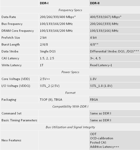
DDR I 和DDR II的简单比较
* Megabit/pin/sec
** The original BL was defined as 4 QW, however, a burst of 8 QW has been added as far as we know per request of Intel/Samsung.
*** DDR I only uses a single DQS, using the cross point with the reference voltage. DDR2 uses a differential DQS as shown on page 3.
+ CAS-3 is possible using a 533 MHz CAS-4 speed bin in DDR400 mode.
++ All current DDR I components are running at 1.8V internally, using voltage regulators to reduce VDD from 2.5V to 1.8V.
+++ Additive Latency can be 0,1,2,3,4T, the actual Read Latency is the sum of CAS latency and Additive Latency, e.g. CAS-4 + AL-4 =8T Read Latency.
posted on 2012-06-15 15:16 freshair_cn 阅读(371) 评论(0) 编辑 收藏 举报


