FPGA-HPS
最近在做DE1的图像方面实验,用到了HPS,所以简要谈一谈什么是HPS.
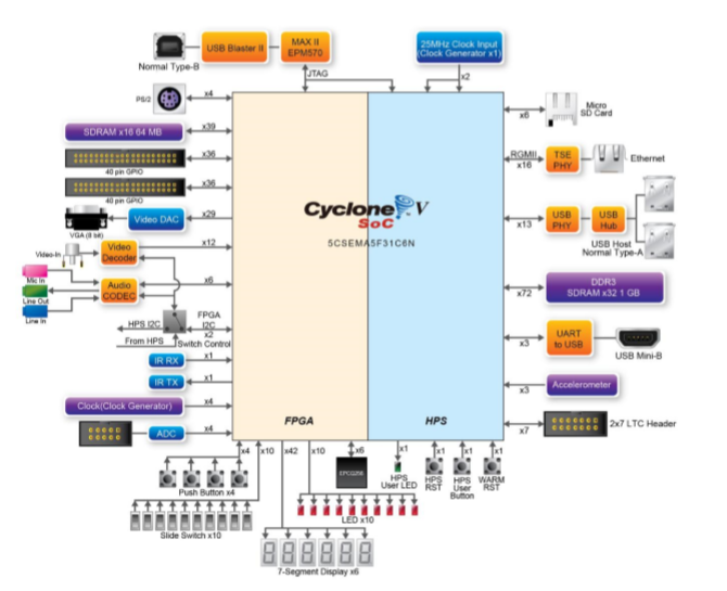
由图可知,DE1的板子就是有fpga+hps组成的;
参考自:http://bbs.eeworld.com.cn/thread-454766-1-1.html
1、HPS:Hard processor system 字面意思就是硬件处理器系统,应该指的是和arm核相连的硬件接口。
2、包括以下内容:
1)Single or dual-core ARM Cortex-A9 MPCore processor-up to 800 MHz maximum frequency with support for symmetric and asymmetric multiprocessing
支持一个或2个ARM Cortex-A9,频率最大能达到800MHz,两个处理器还可以设置成不同的处理速率,这点不知道有什么好处。
2)Interface peripherals —10/100/1000 Ethernet media access control (EMAC), USB 2.0
On-The-GO (OTG) controller, quad serial peripheral interface (QSPI) flash controller,
NAND flash controller, Secure Digital/MultiMediaCard (SD/MMC) controller, UART,
controller area network (CAN), serial peripheral interface (SPI), I2C interface, and
up to 85 HPS GPIO interfaces
接口外设,这个比较好理解,都是常见的arm接口,网口、USB,SPI等等
3)System peripherals —general-purpose timers, watchdog timers, direct memory access
(DMA) controller, FPGA configuration manager, and clock and reset managers
系统外设,这个也比较好理解,就是系统能不运行,而不和外界打交道的,比如定时器,看门狗,DMA控制器等
4) On-chip RAM and boot ROM
片上的RAM和POM,这个还不知道是什么玩意
5)HPS –FPGA bridges —include the FPGA-to-HPS, HPS-to-FPGA, and lightweight
HPS-to-FPGA bridges that allow the FPGA fabric to issue transactions to slaves in
the HPS, and vice versa
这个是比较关键的地方,HPS-FPGA之间的沟通机制
6)FPGA-to-HPS SDRAM controller subsystem —provides a configurable interface to
the multiport front end (MPFE) of the HPS SDRAM controller
接到HPS的SDRAM控制器,应该是和ARM的存储资源有联系
7)ARM CoreSight™ JTAG debug access port, trace port, and on-chip trace storage
这应该说的是调试接口和调试机制
以前的简要介绍
https://www.cnblogs.com/fcfc940503/p/10438350.html

 浙公网安备 33010602011771号