Real time CD quality audio compression and transmission via adaptive differential pulse code modulation
2022-12-07 21:45 dreamboy2000 阅读(77) 评论(0) 收藏 举报With the emergence of Internet of Things, it has become easier than ever to transmit data across embedded systems. More and more modules are designed to enable fast and reliable wireless transmission of data, such as Bluetooth, WiFi, and WiFi-Direct. A valuable use case of these systems is audio transmission. With the Microchip PIC32 that the ECE 4760 course is using this year, we have enough processing power to transmit high-resolution audio data. However, wireless transmission bandwidth and power consumption are still two major limiting factors. To tackle this issue, we can exploit the fact that it is possible to compress audio data such that the human ear can barely discern the difference between original and compressed version. In real time, we can apply signal processing techniques to reduce the size of audio data without losing a significant amount of audio quality, thus allowing audio to be transmitted under relatively strict transmission bandwidth and power consumption constraints.
As our final project, we have explored a particular compression scheme, Adaptive Differential Pulse Code Modulation (ADPCM). ADPCM is capable of a 4:1 compression ratio, which significantly reduces the transmission size. We have designed and constructed separate transmitter and receiver modules. The transmitter samples audio, compresses the resulting digital data, and transmits it to the receiver over SPI. The receiver then decompresses the data and interpolates it to reconstruct the audio signal. In order to preserve the quality of the original audio signal and isolate the effects of ADPCM, we sample and interpolate with CD quality, i.e. sampling frequency of 44.1kHz and 16-bit resolution. We have also implemented our system with stereo audio in order to simulate realistic data throughput.
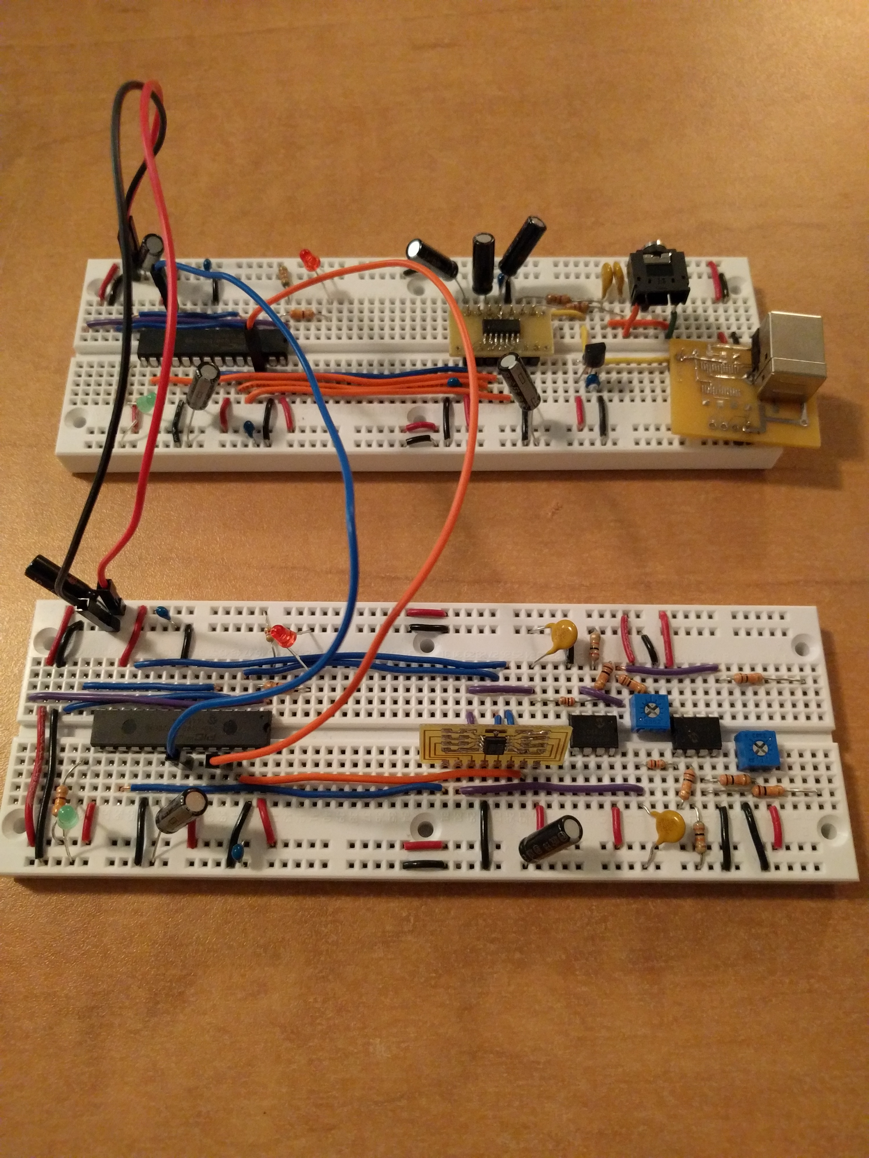
Figure 1: BoomBox hardware
High Level Design top
Rationale
The original project idea is to build a system that is able to turn any wired headsets or speakers wireless. Due to difficulties interfacing with our WiFi module, we decided to use wired data transmission and instead focused on real-time compression techniques, while still keeping the software infrastructure highly modular in such a way that if we were able to successfully interface with the WiFi driver, it would be easy to incorporate wireless transmission into the project.
Logical Structure
At a high level, the system is divided into two main modules, the transmitter and receiver. The transmitter takes in input from an audio source, converts the signal into digital data using an analog-to-digital convert, compresses the data on a PIC32 using Adaptive Differential Pulse Code Modulation, and transmits the compressed data to a different PIC32 receiver. The receiver decompresses the data, sends it to a digital-to-analog converter using I2S, and outputs to an audio device.
Figure 2: System architecture
Background Math
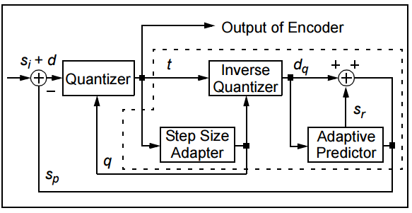
Adaptive Differential Pulse Code Modulation is the algorithm we used for compressing audio data. The ADPCM takes advantage of correlation between consecutive audio samples. While ADPCM is mostly intended for speech samples, it still works relatively well on any kind of audio sample. Similar Differential Pulse Code Modulation, ADPCM is based off the change in audio samples rather than the absolute sample values. However, the advantage of ADPCM is that it varies the quantization step over time, allowing it to easily handle sound with high variation and sound with low variation.
The algorithm utilizes two main states: a predictor and the current quantization step. The predictor represents the previous predicted value. The quantization step represents how far apart two audio samples are from another. At each compression step, the algorithm calculates the difference between the current sample and the predicted sample. It then encodes that difference as a multiple of the quantization step up to a certain point. This means that as the quantization step gets larger, we get less accurate with our measurements. After this, the quantization step is updated based on how far the difference was. If the difference was too big and surpassed the current quantization step, then we increase the step size. Otherwise, we decrease. This part allows the algorithm to adaptively change its encoding based on how varying the audio signal is.
Hardware/Software Tradeoffs
All of our audio sampling and interpolating is done in hardware with external ADC and DAC. Since the audio signal must be scaled and shifted before sampling, we implemented the module for this purpose in hardware. Another added benefit of this approach is that it leaves our MCU with only data compression and transmission, which increases processing speed and reduces distortion. If we wanted to increase the processing speed further, we could offload data compression to a dedicated chip. However, this will potentially increase cost, and there isn't a significant performance gain.
Standards
Audio input and output are designed to use 3.5mm audio jacks (either mono or stereo), and the power supply to the system must be 3.3V. We have heavily used the SPI and I2S protocols.
The Serial Peripheral Interface (SPI) protocol is a full duplex synchronous communcation protocol used for communcating data between two chips. It relies on one of the two chips being a master and supplying an SCLK clock and the other chip being the slave accepting this clock. The MOSI and MISO lines are used to transmit data between the two chips. Data is transmitted in sync with the clock cycles of SCLK.

Figure 3: SPI Bus with 1 slave and 1 master
The Integrated Interchip Sound (I2S) protocol is a communcation protocol for connecting digital audio devices together. It is commonly based on SPI as it usually requires an SCLK. In addition, this protocol also requires an LRCLK and a master clock (MCLK). LRCLK represents the word clock, or the clock cycles that we feed each audio sample in with. MCLK is typically 256 times as fast as LRCLK.

Figure 4: I2S Protocol
Existing Patents
There exists a few patents related to ADPCM, but the claims are implementation-specific, and our project is substantially different from any related patents we could find. To the best of our knowledge, we do not infringe any patent laws, nor do we use any copyrighted or trademarked materials.
Hardware Design top
Audio Input Circuit
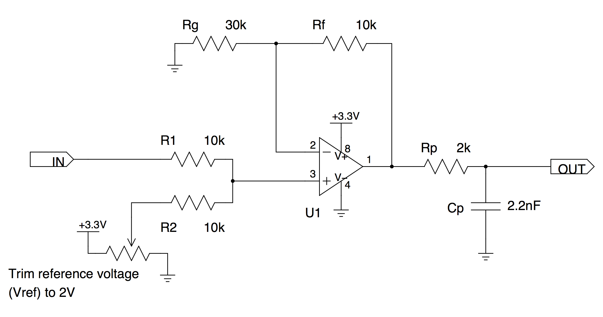
According to our measurements, the audio signal driven by a computer sound card typically ranges from -2V to 2V. However, our ADC is only capable of sampling within the rail-to-rail voltage, which is from 0V to 3.3V. Because of this, it is necessary to construct a circuit that decreases the amplitude and applies a DC offset to the input signal. In other words, we need an an attentuator with a positive DC offset. We have decided to use a non-inverting op amp with a summing circuit on the positive pin.
As shown in Figure 10 in Appendix A, R1 and R2 form a summing circuit, thus adding Vref to the input signal. The sum is then passed into the non-inverting circuit, and the output is low passed to remove noise. Let A be the desired gain, and b be the desired DC offset. Then the following relations can be obtained:
![]()
![]()
In order to convert the signal range from (-2V, 2V) to (0V, 3.3V), we need to set A = 3.3 / (2 - (-2)) = 0.825, and b = 3.3 / 2 = 1.65V. By picking R1 = 10kΩ and Rf = 20kΩ and Vref = 2V, we get R2 = 10kΩ and Rg = 30769Ω. In the end, we have decided on the following values:
| R1 | R2 | Rf | Rg | Vref | A | b |
| 10kΩ | 10kΩ | 10kΩ | 30kΩ | 2V | 0.667 | 1.333V |
Lastly, we have included a first-order low-pass filter to remove noise before sampling.
Analog-to-Digital Converter
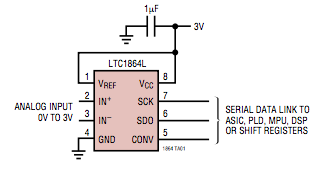
The PIC32 on-chip ADC does not have enough resolution to provide CD quality, and our ADC needs to support two channels in order to create stereo sound. As such, we have chosen to use the LTC1865L, a 16-bit, dual-channel ADC. This chip is capable of supporting up to 150k samples per second, more than enough for our 44.1kHz requirements.
Digital-to-Analog Converter
Similar to our ADC constraints, our DAC also needs to support two channels and CD quality. From our research, it seems that DACs that achieve CD quality often require more fine control. As a result, we aimed for a chip that is simple to work with. We have chosen the CS4354 under these constraints. This chip required the I2S protocol for digital data input, which the PIC32 conveniently provides. It also requires a separate 5V source, which we have provided using USB power. The output of each DAC channel is then low-passed to remove noise.
Software Design top
Transmitter Software Architecture
There are four main components within the transmitter program: ADC Reading, compression, ring buffer and data transmission. This program consists of the main loop and an ISR that handles audio input. The ISR is timer driven and reads the current audio value from the ADC at a 44.1kHz sampling rate. At the same time, the main loop waits until we have a continuous range of 256 samples from both the left and right ears and then it transmits them in a batch.
Receiver Software Architecture
Similar to the transmitter side, there are four main components within the receiver program: data reception, ring buffer, decompression, and DAC output. Data reception is executed within the main loop, and blocks on SPI read. Once a data packet is read, it is then unpacked and pushed into the ring buffer. A separate I2S-based ISR handles decompressing the data and writing to the DAC.
Adaptive Differential Pulse Code Modulation
Our ADPCM code is heavily based off of Microchip's sample code in their AppNote. As mentioned in the math background, we keep track of both the predictor and the quantization step for both the left and right ear individually. This is because the audio streams are independent and we don't want to correlate them together.
On the encoding side, we take in a 16 bit audio sample and generate a 4 bit encoded value. The most significant bit of the four bits determines the sign of the delta. If it is 1, then are current audio sample is smaller than the previously predicted sample. Otherwise, the audio sample is higher than the previously predicted sample. The remaining 3 bits represents how many quantization steps the difference is. If the remaining 3 bits is greater than or equal to 0b100, then we want to increase our quantization step. Otherwise, we decrease the quantization step.
Figure 5: ADPCM Encoding
The decoding side does the same as the encoding side but in reverse. It takes in a 4 bit encoded value and outputs the 16 bit decoded audio sample. It achieves this by recalculating the delta off the predicated value and adding that the predicted value. The quantization step change is calculated in the same way as in encoding.
Figure 6: ADPCM Decoding
ADC Read
We used the SPI protocol in order to communicate with our ADC. We use the transmitter MCU as master and the LTC1865L as slave. As the LTC1865L provides stereo input, we alternate between requesting for the left and right audio signal. In order to tell the ADC which side to read from, we send two configuration bits and then read the response. As per the datasheet, 0b10 is sent to request the left channel which 0b11 is sent to request the right channel.
We read audio data on a timer interrupt set to 88.2kHz. The timer is set to twice the audio sampling rate in order to support both left and right side. On timer interrupt, we alternate sides and then compress and store the audio data into a ring buffer. We compress before storing in order to reduce the amount of memory required. One caveat of this approach is that the left and right audio signals will be desynchronized by just over 11µs. However, such a small lag is completely undetectable by the human ear.
DAC Write
We used the I2S protocol in order to communicate with the DAC. The PIC32 supports this protocol as an extra setting on the SPI channels that it provides. We use the receiver MCU as master and provide SCLK, MCLK, and LRCLK entirely from the MCU. While the CS4354 chip is able to produce an internal SCLK, we discovered that the internal SCLK often caused desynchronization issues.
As per the I2S specifications, we used an LRCLK with a frequency of 44.1kHz. We also used the REFCLK output of the PIC32 to act as MCLK, generating an 11.2896 MHz clock. On every LRCLK edge, we pull the next audio signal from the ring buffer, decompress it and send it to the DAC. Once again, we alternate left and right resulting in the same audio desynchronization as in the ADC. Because the DAC we use supports up to 24 bits resolution, we left shift our audio signal by 8 in order to mask it as a 24 bit number.
Ring Buffer
We utilize a ring buffer in order to continuously buffer the audio input and output of the chip. The ring buffer acts as FIFO queue that allows us to maintain the ordering of the audio data stream. This also allows us to buffer a large list of samples before we transmit them all in a single packet. On the receiving side, the ring buffer allows us to buffer the packets that come in to later be outputted to the DAC.
Data Transfer
We used the SPI protocol for data transmission between the transmitter and receiver. The transmitter MCU is set as master, and the receiver MCU is set as slave. Each data packet contains 256 bytes, where each byte correspond to a single unit of compressed data containing information from both left and right audio channels. In order to identify packet boundaries, we standardized on a 4-byte sync word, which is constructed by taking a single-byte constant and repeating it four times. The sync word is not strictly necessary in our current setup since the receiver can pick up any consecutive 256 bytes and view that as a packet. However, we designed the system with potential wireless usage in mind, and the sync word very roughly mimics a UDP packet header. The transmitter continuously transmits packets without any acknowledgement from the receiver, since doing so may accumulate delay over time without much performance benefit. On the other hand, the receiver does not proceed to push to the ring buffer until a packet header is recognized.
Results top
Sound Quality and Accuracy
In order to isolate the performance of our compression scheme, we must ensure that the audio input circuit produces a signal that has nearly the same waveform as the audio input, with the exception of amplitude and offset. Figures 7 shows that the circuit operates as expected for both left and right channels while audio is playing, and Figures 8 demonstrate the expected DC offset while there is no audio.
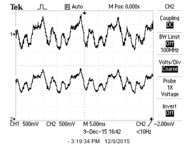
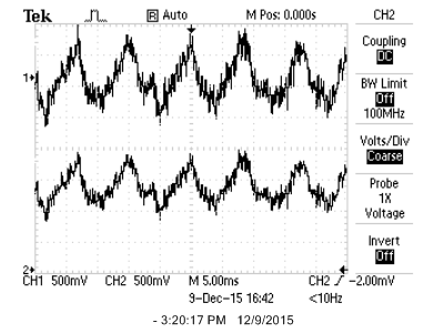
Figure 7: Typical audio signal comparison for left channel (left) and right channel (right). CH1 is the audio source, and CH2 is the output of the op-amp audio input circuit.
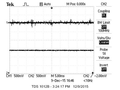
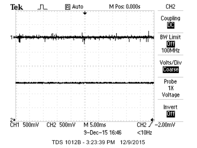
Figure 8: Signal comparison for left channel (left) and right channel (right), with no sound. CH1 is the audio source, and CH2 is the output of the op-amp audio input circuit.
Figures 9 shows the comparison between audio input and the final output of the system. Note that very frequently, ADPCM causes the output to overshoot, but quickly returns to the correct value. This is the adaptive part of the algorithm at work: the system tries to maintain the previous increment, but the input drastically changes, and in response, the algorithm changes the increment by a large value to compensate for this. Another observation is that the scale of the output is set to 100mV per grid, instead of 500mV per grid, so amplitude is not preserved.
In terms of sound quality, overall the output very closely resembles the audio input. There is a slight detectable noise in the background, which may be due to oscillations in the power line. Another bug is that when the system starts, the output is very quiet. Over time, the volume suddenly boosts up at sporadic times. This is related to the difference in amplitude scale mentioned above. Due to time constraints, we were unable to investigate into this issue, but we suspect that it could be related to overflow or underflow in the ADPCM algorithm implementation.
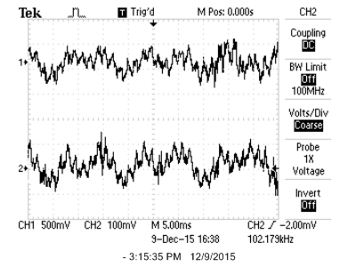
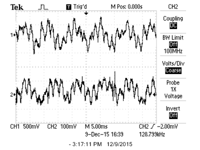
Figure 9: Typical audio signal comparison for left channel (left) and right channel (right). CH1 is the audio source, and CH2 is the final system output.
Speed of Execution
There is no audible delay between the audio input and audio output, so we were able to reach our performance goals. We have also allowed the system to run for a long period of time in order to test whether there are small delays that accumulate to larger delays over time, but there is still no audible discrepancy. As shown in Figure 9, the right channel has a slight millisecond delay, but this is not audible.
Conclusions top
Our final result did meet our original expectation of being able to transmit compressed audio. We were also able to meet the goal of transmitting CD quality sound at stereo 44.1kHz, 16 bit resolution. Our compression scheme yielding a compression ratio of 4:1 with very little noticeable degredation of sound quality. However, we were unable to extend the transmission protocol to the wireless domain due to time constraints.
Further Work
Further work that can be done in this project include exploring different audio compression methods. We want to be able to compress audio in real time on a relatively low processing power chip. To do so, we can look at other methods of real time audio compression. For example, Opus is currently one of the leading real time audio codecs. Boasting a low algorithmic delay of around 25ms, Opus is currently being used in many commercial VOIP programs such as Skype, Mumble, Teamspeak, etc. Additionally, Opus utilizes subcodecs, CELT and SILK, in order to compress music and speech audio, allowing it to maintain quality for both music and speech. If Opus proves to be too algorithmically intensive to run on a PIC32, we can look further into either CELT or SILK.
Because our transmission protocol utilizes a packet based transmission scheme, we can easily extend this to work across other types of channels. For this project, we transmit packets over SPI to another PIC32, but we could swap the SPI protocol out for either Bluetooth or WiFi. These protocols would enable us to transmit our audio data wirelessly between two microcontrollers, creating an end to end wireless audio communication protocol.
Intellectual Property Considerations
Excluding the ADPCM code, the code used for this project was entirely written by us. While we used a few pieces of sample code from Microchip as reference, we ultimately wrote everything ourselves.
A portion of the ADPCM code was taken from the AppNote from Microchip. However, in order to get it to work on the PIC32 we were using, we had to modify the sample code. The AppNote for ADPCM has a Software License Agreement that states that the sample code is intended to only be used with products manufactured by Microstick. We have abided by this license as the PIC32 was manufactured by Microstick.
Ethical Considerations
We designed this project keeping in mind the IEEE Code of Ethics.
We did not utilize any harmful materials in the construction of our project. Additionally, our final product was constructed keeping in mind human safety. Neither the transmitter nor receiver were designed to cause any hard to humans. All of our hardware runs at low current at either 3.3V or 5V. The current will not harm a user even if he touched the exposed wiring. If we were to construct this device to be sold rather than as a prototype, we would remove the use of whiteboards to reduce the wiring exposed to the end user. Additionally, as the receiver and transmitter modules are self contained, we could add a casing for both modules for further safety.
Our project is designed to be able to be used by anyone. This means that even people with disabilities will be able to utilize our project.
All work in this project stated as independent work was done entirely by ourselves. We have also including references to all of the datasheets, figures, and additional information we have utilized in the Appendices and References sections. We certify that we have openly disclosed anyone else's work we have used in this project.
Legal Considerations
There are no legal consideration as far as we know of. There are not legal regulations associated with either the SPI or I2S protocols.
Appendices top
A. Schematics
Figure 10: Audio input schematic
Figure 11: ADC Schematics. Source: LTC1865L datasheet. Note: the LTC1865L schematic is identical to the LTC1864, with the exception of the IN+ and IN- pins replaced by CH0 and CH1.
Figure 12: DAC Schematics. Source: CS4354 datasheet. Actual component values differ slightly due to lab supply limits.
B. Cost & Parts List
| Part Number | Vendor | Quantity | Price | Total Cost |
| PIC32MX250F128B | Lab stock | 2 | $5.00 | $10.00 |
| Breadboard | Lab stock | 2 | $6.00 | $12.00 |
| LTC1865L ADC | Linear Technology | 1 | Sampled | $0.00 |
| CS4354 DAC | Cirrus Logic | 1 | Sampled | $0.00 |
| MCP6242 Op Amp | Lab stock | 2 | $0.00 | $0.00 |
| Trimpot | Lab stock | 2 | $0.00 | $0.00 |
| 5V Power Connector (USB) | Lab stock | 1 | $0.00 | $0.00 |
| Assorted Resistors, Capacitors and LEDs | Lab stock | As Used | $0.00 | $0.00 |
| Total: | $22.00 | |||
C. Distribution of Work
| Cheng Xing | Rene Zhang |
|---|---|
| Hardware Design & Implementation | Software Design & Implementation |
| Audio Input Design & Implementation | ADPCM Research & Implementation |
| Receiver Code | Transmitter Code |
| Testing | Testing |
| Website | Website |
D. Code Listing
Transmitter code:
Receiver code:
ADPCM code:
Ring Buffer code:




 浙公网安备 33010602011771号