


GTP+SDI工程播出部分思路整理
1.video_out_to_sdi模块
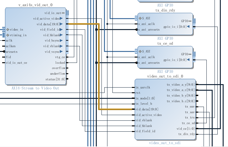
关于video_out_to_sdi模块的输出信号:
tx_video_a_y[9:0]
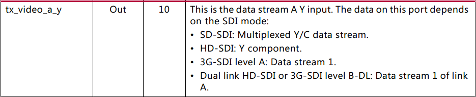
这是要输入SDI IP核内的
tx_video_a_c[9:0]
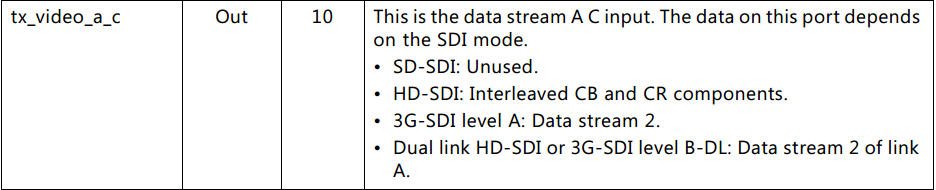
同样是要输入给SDI 核内的,需要重点关注SDI播出工程中有关这两个信号线的连接情况。
tx_ce_sd
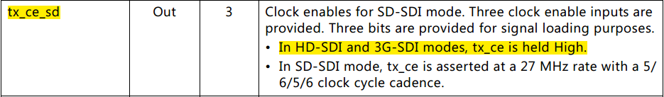
时钟使能
Vid_ce[1:0]

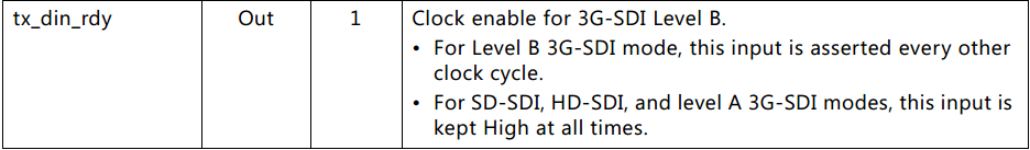
Tx_din_rdy
2.SDI工程
查阅x7gtx_sdi_wrapper模块:

module x7gtx_sdi_wrapper #(
    parameter FXDCLK_FREQ               = 27000000,     // Frequency, in hertz, of fixed frequency clock
    parameter DRPCLK_PERIOD             = 13,           // Period of drpclk in ns, always round down
    parameter PLLLOCK_TIMEOUT_PERIOD    = 2000000,      // Period of PLLLOCK timeout in ns, defaults to 2ms
    parameter RESET_TIMEOUT_PERIOD      = 500000,       // Period of GTH RESETDONE timeout in ns, defaults to 500us
    parameter TIMEOUT_CNTR_BITWIDTH     = 15,           // Width in bits of timeout counter
    parameter RETRY_CNTR_BITWIDTH       = 8,            // Width in bits of the retry counter
    parameter CPLL_REFCLK_PORT          = "REFCLK1",    // Options are REFCLK0, REFCLK1, GREFCLK, NORTH0, NORTH1, SOUTH0, SOUTH1
    parameter TX_CLK0_QPLL              = 1,            // Set to 1 if QPLL is TX serial clock source with tx_m = 0, else set to 0
    parameter TX_CLK1_QPLL              = 0,            // Set to 1 if QPLL is TX serial clock source with tx_m = 1, else set to 0
    parameter GT_SIM_GTRESET_SPEEDUP    = "FALSE")
(
    input   wire        clk,                    // fixed frequency clock for GTX control module
    input   wire        drpclk,                 // DRPCLK
    input   wire        qpllclk,                // connect to the GTXE2_COMMON qplloutclk
    input   wire        qpllrefclk,             // Connect to the GTXE2_COMMON qplloutrefclk
    output  wire        qpllreset,
    input   wire        qplllock,
    input   wire        cpllrefclk,
    output  wire        cplllock,
    input   wire        rxp,
    input   wire        rxn,
    output  wire        txp,
    output  wire        txn,

// RX ports
    input  wire         rx_rst,                 // sync reset for SDI RX pipeline
    output wire         rx_usrclk_out,          // rxusrclk input
    input  wire         rx_gtx_full_reset,      // 1 causes a full reset of GTX RX, including the QPLL                  (drpclk)
    input  wire         rx_gtx_reset,           // 1 causes a GTRXRESET cycle to occur                                  (drpclk)
    input  wire         rx_refclk_stable,       // input must be low until reference clock to QPLLis stable             (async)
    input  wire         rx_frame_en,            // 1 = enable framer position update
    input  wire [2:0]   rx_mode_en,             // unary enable bits for SDI mode search {3G, SD, HD} 1=enable, 0=disable
    output wire [1:0]   rx_mode,                // 00=HD, 01=SD, 10=3G
    output wire         rx_mode_hd,             // 1 = HD mode
    output wire         rx_mode_sd,             // 1 = SD mode
    output wire         rx_mode_3g,             // 1 = 3G mode
    output wire         rx_mode_locked,         // auto mode detection locked
    output wire         rx_bit_rate,            // 0 = 1000/1000, 1 = 1000/1001
    output wire         rx_t_locked,            // transport format detection locked
    output wire [3:0]   rx_t_family,            // transport format family
    output wire [3:0]   rx_t_rate,              // transport frame rate
    output wire         rx_t_scan,              // transport scan: 0=interlaced, 1=progressive
    output wire         rx_level_b_3g,          // 0 = level A, 1 = level B
    output wire         rx_ce_sd,               // clock enable for SD, always 1 for HD & 3G
    output wire         rx_nsp,                 // framer new start position
    output wire [10:0]  rx_line_a,              // line number for HD & 3G (link A for level B)
    output wire [31:0]  rx_a_vpid,              // payload ID packet ds1 for 3G or HD-SDI
    output wire         rx_a_vpid_valid,        // 1 = rx_a_vpid is valid
    output wire [31:0]  rx_b_vpid,              // video payload ID packet data from data stream 2
    output wire         rx_b_vpid_valid,        // 1 = rx_b_vpid is valid
    output wire         rx_crc_err_a,           // CRC error for HD & 3G
    output wire [9:0]   rx_ds1a,                // data stream 1A: SD=Y/C, HD=Y, 3GA=ds1, 3GB=Y link A
    output wire [9:0]   rx_ds2a,                // data stream 2A: HD=C, 3GA=ds2, 3GB=C link A
    output wire         rx_eav,                 // 1 during XYZ word of EAV
    output wire         rx_sav,                 // 1 during XYZ word of SAV
    output wire         rx_trs,                 // 1 during all 4 words of EAV and SAV
    output wire [10:0]  rx_line_b,              // line number of 3G level B link B
    output wire         rx_dout_rdy_3g,         // 3G data ready: 1 for level A, asserted every other clock for level B
    output wire         rx_crc_err_b,           // CRC error for link B (level B only)
    output wire [9:0]   rx_ds1b,                // data stream 1B: 3G level B only = Y link B
    output wire [9:0]   rx_ds2b,                // data stream 2B: 3G level B only = C link B
    input  wire [15:0]  rx_edh_errcnt_en,       // enables various errors to increment rx_edh_errcnt
    input  wire         rx_edh_clr_errcnt,      // clears rx_edh_errcnt
    output wire         rx_edh_ap,              // 1 = AP CRC error detected previous field
    output wire         rx_edh_ff,              // 1 = FF CRC error detected previous field
    output wire         rx_edh_anc,             // 1 = ANC checksum error detected
    output wire [4:0]   rx_edh_ap_flags,        // EDH AP flags received in last EDH packet
    output wire [4:0]   rx_edh_ff_flags,        // EDH FF flags received in last EDH packet
    output wire [4:0]   rx_edh_anc_flags,       // EDH ANC flags received in last EDH packet
    output wire [3:0]   rx_edh_packet_flags,    // EDH packet error condition flags
    output wire [15:0]  rx_edh_errcnt,          // EDH error counter
    output wire         rx_change_done,         // 1 indicates resets or dynamic SDI mode changes are complete              (drpclk)
    output wire         rx_change_fail,         // 1 indicates failure of a reset or dynamic SDI mode change                (drpclk)
    output wire [2:0]   rx_change_fail_code,    // if rx_change_fail is 1, this port indicates reason for failure           (drpclk)
    output wire         drpbusy,                // 1 when the SDI RX control logic is using the GTX DRP                     (drpclk)

// TX ports
    input  wire         tx_rst,                 // sync reset for SDI TX pipeline
    output wire         tx_usrclk_out,          // clock input
    input  wire         tx_gtx_full_reset,      // causes a full reset of the GTH TX including PLL                          (drpclk)
    input  wire         tx_gtx_reset,           // causes a reset of the GTH TX, not including the PLL                      (drpclk)
    input  wire         tx_refclk_stable,       // assert high when reference clock to the TX PLL is stable                 (async)
    input  wire [2:0]   tx_ce,                  // clock enable - 3 identical copies
    input  wire         tx_din_rdy,             // input data ready for level B, must be 1 for all other modes
    input  wire [1:0]   tx_mode,                // 00 = HD, 01 = SD, 10 = 3G
    input  wire         tx_level_b_3g,          // 0 = level A, 1 = level B
    input  wire         tx_m,                   // 0 = select 148.5 MHz refclk, 1 = select 148.35 MHz refclk
    input  wire         tx_insert_crc,          // 1 = insert CRC for HD and 3G
    input  wire         tx_insert_ln,           // 1 = insert LN for HD and 3G
    input  wire         tx_insert_edh,          // 1 = generate & insert EDH for SD
    input  wire         tx_insert_vpid,         // 1 = enable ST352 PID packet insert
    input  wire         tx_overwrite_vpid,      // 1 = overwrite existing ST352 packets
    input  wire [9:0]   tx_video_a_y_in,        // Data stream Y link A input: SD Y/C, HD & 3GA Y in, 3GB A Y in
    input  wire [9:0]   tx_video_a_c_in,        // Data stream C link A input: HD & 3GA C in, 3GB A C in
    input  wire [9:0]   tx_video_b_y_in,        // 3G level B only: Data stream Y link B input
    input  wire [9:0]   tx_video_b_c_in,        // 3G level B only: Data stream C link B input
    input  wire [10:0]  tx_line_a,              // current line number for link A
    input  wire [10:0]  tx_line_b,              // current line number for link B
    input  wire [7:0]   tx_vpid_byte1,          // ST352 user data word 1
    input  wire [7:0]   tx_vpid_byte2,          // ST352 user data word 2
    input  wire [7:0]   tx_vpid_byte3,          // ST352 user data word 3
    input  wire [7:0]   tx_vpid_byte4a,         // ST352 user data word 4 for link A
    input  wire [7:0]   tx_vpid_byte4b,         // ST352 user data word 4 for link B
    input  wire [10:0]  tx_vpid_line_f1,        // insert ST352 packet on this line in field 1
    input  wire [10:0]  tx_vpid_line_f2,        // insert ST352 packet on this line in field 2
    input  wire         tx_vpid_line_f2_en,     // enable ST352 packet insertion in field 2
    output wire [9:0]   tx_ds1a_out,            // data stream 1, link A out
    output wire [9:0]   tx_ds2a_out,            // data stream 2, link A out
    output wire [9:0]   tx_ds1b_out,            // data stream 1, link B out
    output wire [9:0]   tx_ds2b_out,            // data stream 2, link B out
    input  wire         tx_use_dsin,            // 0=use the internal data streams, 1=use the tx_dsxx_in data streams
    input  wire [9:0]   tx_ds1a_in,             // data stream 1 link A in: SD Y/C, HD Y, 3G Y, dual-link A Y
    input  wire [9:0]   tx_ds2a_in,             // data stream 2 link A in: HD C, 3G C, dual-link A C
    input  wire [9:0]   tx_ds1b_in,             // data stream 1 link B in: dual-link B Y
    input  wire [9:0]   tx_ds2b_in,             // data stream 2 link B in: dual-link B C
    output wire         tx_ce_align_err,        // 1 if ce 5/6/5/6 cadence is broken
    output wire         tx_slew,                // slew rate control signal for SDI cable driver
    output  wire        tx_change_done,         // 1 when txrate or txsysclksel changes complete successfully               (drpclk)
    output  wire        tx_change_fail,         // 1 when txrate or txsysclksel changes fail                                (drpclk)
    output  wire [2:0]  tx_change_fail_code     // failure code when tx_change_fail = 1                                     (drpclk)
);
TX ports部分信号定义如下:
input  wire         tx_rst,                 // sync reset for SDI TX pipeline

output wire         tx_usrclk_out,          // clock input

input  wire [2:0]   tx_ce,                  // clock enable - 3 identical copies

input  wire         tx_din_rdy,             // input data ready for level B, must be 1 for all other modes

input  wire [1:0]   tx_mode,                // 00 = HD, 01 = SD, 10 = 3G

input  wire         tx_level_b_3g,          // 0 = level A, 1 = level B

input  wire [9:0]   tx_video_a_y_in,        // Data stream Y link A input: SD Y/C, HD & 3GA Y in, 3GB A Y in

input  wire [9:0]   tx_video_a_c_in,        // Data stream C link A input: HD & 3GA C in, 3GB A C in

output wire [9:0]   tx_ds1a_out,            // data stream 1, link A out

output wire [9:0]   tx_ds1b_out,            // data stream 1, link B out

input  wire [9:0]   tx_ds1a_in,             // data stream 1 link A in: SD Y/C, HD Y, 3G Y, dual-link A Y

input  wire [9:0]   tx_ds1b_in,             // data stream 1 link B in: dual-link B Y
这是需要重点关注的。
本工程播出部分的视频数据是通过工程内部的video pattern generators来产生
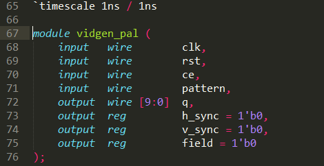
//------------------------------------------------------------------------------
// Video pattern generators
//
multigenHD VIDGEN (
    .clk                (tx_usrclk),
    .rst                (tx_fabric_reset),
    .ce                 (1'b1),
    .std                (tx_fmt),
    .pattern            (tx_pat),
    .user_opt           (2'b00),
    .y                  (tx_hd_y),
    .c                  (tx_hd_c),
    .h_blank            (),
    .v_blank            (),
    .field              (),
    .trs                (),
    .xyz                (),
    .line_num           (tx_line));

vidgen_ntsc NTSC (
    .clk                (tx_usrclk),
    .rst                (tx_fabric_reset),
    .ce                 (tx_sd_ce),
    .pattern            (tx_pat[0]),
    .q                  (tx_ntsc_patgen),
    .h_sync             (),
    .v_sync             (),
    .field              ());

vidgen_pal PAL (
    .clk                (tx_usrclk),
    .rst                (tx_fabric_reset),
    .ce                 (tx_sd_ce),
    .pattern            (tx_pat[0]),
    .q                  (tx_pal_patgen),
    .h_sync             (),
    .v_sync             (),
    .field              ());
因此,只需要弄懂video pattern generators 与SDI播出部分是怎么连接的,就可以摸索出video_out_to_sdi 模块应该怎样与SDI工程连接。
1.tx_video_a_y_in信号连接路径:
.tx_video_a_y_in (tx_y),
assign tx_y = tx_mode == 2'b01 ? tx_sd : tx_hd_y;
可以得出当 tx_mode == 2’b01的时候,tx_y 为tx_sd;
当tx_mode 不为2’b01的时候,tx_y 为 tx_hd_y;
所以,现在需要找到tx_sd 和 tx_hd_y信号线在哪里。
assign tx_sd = tx_fmt[0] ? tx_pal_patgen : tx_ntsc_patgen;
则,tx_sd 根据tx_fmt[0]的值,来决定是为tx_pal_patgen 还是为tx_ntsc_patgen;
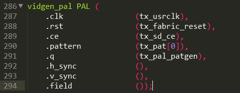
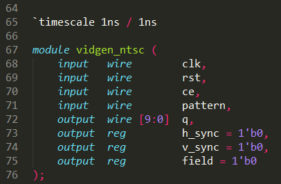
产生PAL视频数据,查看vidgen_pal模块代码中q信号的定义。

综合以上分析可以得出tx_y信号是视频输出信号,然后输入给SDI TX端口的tx_video_a_y_in
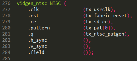
产生NTSC 视频数据,查看vidgen_ntscl模块代码中q信号的定义

综合以上分析可以得出tx_y信号是视频输出信号,然后输入给SDI TX端口的tx_video_a_y_in
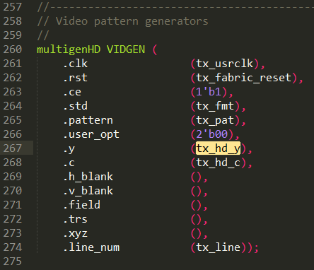
产生multigenHD视频数据,查看multigenHD模块代码中y信号的定义
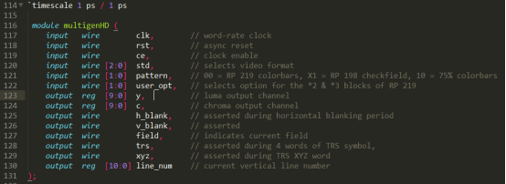
则y为luma数据.(YUV)
综合以上分析可以得出tx_y信号是视频输出信号(luma),然后输入给SDI TX端口的tx_video_a_y_in
(未完,continue......)

【推荐】国内首个AI IDE,深度理解中文开发场景,立即下载体验Trae
【推荐】编程新体验,更懂你的AI,立即体验豆包MarsCode编程助手
【推荐】抖音旗下AI助手豆包,你的智能百科全书,全免费不限次数
【推荐】轻量又高性能的 SSH 工具 IShell:AI 加持,快人一步
· 10年+ .NET Coder 心语,封装的思维:从隐藏、稳定开始理解其本质意义
· .NET Core 中如何实现缓存的预热?
· 从 HTTP 原因短语缺失研究 HTTP/2 和 HTTP/3 的设计差异
· AI与.NET技术实操系列:向量存储与相似性搜索在 .NET 中的实现
· 基于Microsoft.Extensions.AI核心库实现RAG应用
· 10年+ .NET Coder 心语 ── 封装的思维:从隐藏、稳定开始理解其本质意义
· 地球OL攻略 —— 某应届生求职总结
· 提示词工程——AI应用必不可少的技术
· Open-Sora 2.0 重磅开源!
· 周边上新:园子的第一款马克杯温暖上架