HDLBits_Verilog学习笔记Ⅰ——Verilog Language_Basics
作者:脱发秘籍搬运工 https://www.bilibili.com/read/cv10338711?spm_id_from=333.999.0.0 出处:bilibili
Verilog在线学习网站:HDLBits
2. Simple wire
小知识点:
与现实中的导线不同,Verilog中的wire是一种信号,和其余信号一样,它是有方向性的。其承载的信息值只向一个方向流动,通常从一个source流向一个或多个sinks(source“源”也常被称为driver“驱动”,它将某个值驱动至导线上)。
在Verilog中,“连续赋值”(assign left_side = right_side; )将wire信号right_side的值驱动至左边的wire信号left_side。由于赋值是“连续的”(即连了一根导线),所以right_side的任何变化都会立即在left_side中体现出来。
这与软件的赋值不同,连续赋值不是一次性事件。
模块上的端口也有方向性(通常是input或output)。输入端口由模块外的信号驱动,而输出端口驱动模块外的信号。从模块内部看时,输入端口是驱动或源,而输出端口是接收器。
浅出:assign left = right; 在现实中就是用一根导线(wire)将两个引脚连起来,电信号从right流向left,所以Verilog里就把right和left定义为wire类型的信号(此外还有reg等),其中right是源或驱动,left是被驱动的sink。
---------------------------------------------------------------------------------------------------------------------------------------------------------------------------------------------------------
Practice: Create a module with one input and one output that behaves like a wire.
大白话:搞一个极简单的电路模块,它有两个端口,一进一出,Verilog中对应两个wire类型的信号,in是source,out是sink,通过assign语句把这两wire信号用一根导线wire连起来。
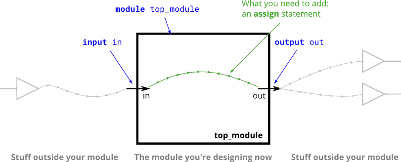
module top_module( input in, output out );

    assign out = in;

endmodule
PS.Verilog在定义input和output时可以省略wire,即相当于(input wire in, output wire out)。
3. Four wires
小知识点:
这道题需要用到不止一条assign语句,而Verilog中的多条assign语句间的顺序是不会影响结果的;这又与按顺序执行的软件代码不同,Verilog是并行的。
另外再重申一遍,图中的绿线是两个wire信号之间的连接,在现实中它可以是一根导线(英语单词wire),但在Verilog中的wire表示的是某一种类型的信号。
浅出:可综合的Verilog代码本质上是在描述现实中的硬件电路,电路中的导线或器件先连后连基本没有区别,硬件系统中的模块也都是相互独立且并行运行的,所以用来描述硬件结构的Verilog也具有并行性(always和initial行为语句块内部的begin...end顺序语句组是顺序执行的,这个后面会细讲)。
----------------------------------------------------------------------------------------------------------------------------------------------------------------------------------------------
Practice: Create a module with 3 inputs and 4 outputs that behaves like wires that makes these connections: a->w,b->x,b->y,c->z.
大白话:用assign语句连线,得注意谁驱动谁。

module top_module(input a,b,c,output w,x,y,z );

    assign w = a;阻塞赋值语句,立刻赋值与仿真时间无关
    assign x = b;
    assign y = b;
    assign z = c;

endmodule
BB两句:上题有提到source通常只有一个,而sinks可以有多个,比如这题的x和y就同时被b驱动。
Why?因为一个wire信号不能被多个信号同时驱动,假设x同时连了a和b,如果a来了个高电平,b来了个低电平,那x是高还是低呢。又如果一个wire信号没有其他信号驱动它,此时综合器会将其默认为0。
4. Inverter
小知识点:
Verilog中有两种取反:逻辑取反 ! 和按位取反 ~ ,前者只能用于一位的信号,即!1=0, !0=1,在电路中对应一个反相器;后者还可用于多位宽的信号,如~101=010。
------------------------------------------------------------------------------------------------------------------------------------------------------------------------------------------------------------------------------------------------------
Practice: Create a module that implements a NOT gate.
大白话:搞一个非门(反相器)。
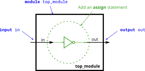
module top_module( input in, output out );

  assign out = !in; //也可以用~

endmodule
5. And gate
小知识点:
与分两种:按位与 & 和逻辑与 && 。
浅出:按位与很简单,就是一位一位地与运算过去,最后产生的输出肯定也是n位的(例如 1011 & 0110 = 0010)。
而逻辑与就是把所有位作为一个整体,只有每一位都为0(整体等于零),它才可记成一位的“0”,不然它整体就不等于零,也就记“1”,最后的输出也仅剩1位(例如 10 && 11=1,10 && 00=0)。
这个在下一篇的13题还会细讲。
------------------------------------------------------------------------------------------------------------------------------------------------------------------------------------------------------------------------------------------------------
Practice: Create a module that implements an AND gate.
大白话:建一个与门。
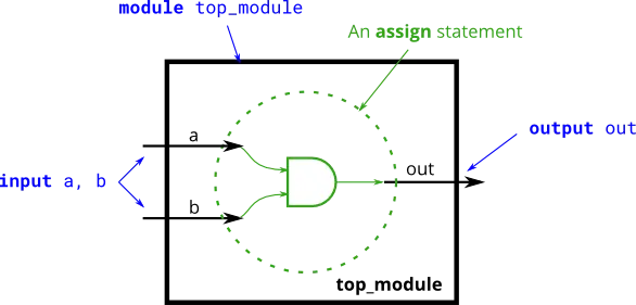
module top_module(input a,input b,output out );

    assign out = a && b; //或用&

endmodule
6. NOR gate
小知识点:或也分两种,按位或 | 和逻辑或 || ,类似上题的与。
------------------------------------------------------------------------------------------------------------------------------------------------------------------------------------------------------------------------------------------------------
Practice: Create a module that implements a NOR gate. A NOR gate is an OR gate with its output inverted. A NOR function needs two operators when written in Verilog.
大白话:或非门包括或门和非门。

module top_module(input a,input b,output out );

    assign out = ~ (a | b);

endmodule
7. XNOR gate
小知识点:异或只有按位异或 ^ ,没有逻辑异或,另外还有个同或运算符 ^~。同或就是异或的非。
------------------------------------------------------------------------------------------------------------------------------------------------------------------------------------------------------------------------------------------------------
Practice: Create a module that implements an XNOR gate.
大白话:XNOR表示同或,XOR是异或。
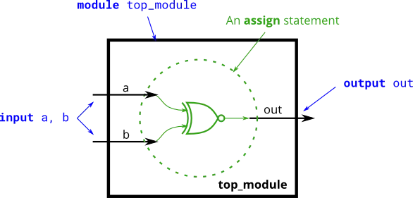
module top_module(input a,input b,output out );

    assign out = ~ (a ^ b);
// 或assign out = a ^~ b;

endmodule
8. Declaring wires
小知识点小知识点:
前面我们对wire信号blabla地讲了一大堆,但是貌似并没有用到过它(input和output除外),那是因为前面的电路太简单了。这次我们就要在模块内定义wire类型的信号,来描述更复杂一丢丢的电路。格式如下 👇
wire your_signal_1, your_signal_2;
------------------------------------------------------------------------------------------------------------------------------------------------------------------------------------------------------------------------------------------------------
Practice: Implement the following circuit. Create two ...
大白话:实现下面的电路,创建两个中间信号把与门和或门连起来。非门的输入信号已经存在(就是out),所以没必要定义第三个中间信号。另外不要忘了上面反复强调的一个wire信号只能由一个信号驱动,但能驱动多个其它信号。
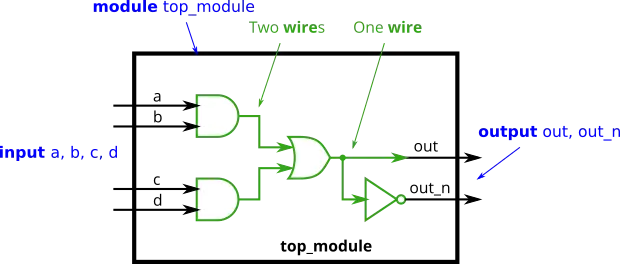
`default_nettype none
module top_module (
input a,
input b,
input c,
input d,
output out,
output out_n );

    wire and1, and2; // wire信号声明时也可直接赋值,这样就能少写一句

    assign and1 = a & b; // 省略上一句后,可改成 wire and1 = a & b;
    assign and2 = c & d; // 省略上一句后,可改成 wire and2 = c & d;

    assign out = and1 | and2;
    assign out_n = ~out;

endmodule
`default_nettype none是一个宏定义,下一篇的11题会讲到。可以在定义wire信号的时候直接赋值(如wire and1 = a & b;),Verilog也支持这种语法。
9. 7458 chip
小知识点:
7458是一款带有四个“与”门和两个“或”门的芯片。
创建一个功能与7458芯片相同的模块。它有10个输入和2个输出。您可以选择使用assign语句来驱动每条输出线,也可以选择声明四条线用作中间信号,其中每条内部线由一个AND门的输出驱动。
----------------------------------------------------------------------------------------------------------------------------------------------------------------------------------------------------------------------------------------------------------------------------------------------------------------
Practice: Create a module with the same functionality as the 7458 chip.
大白话:写一块7458芯片模块,如图所示。
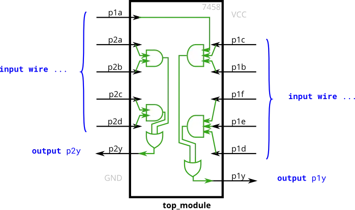
module top_module (
input p1a, p1b, p1c, p1d, p1e, p1f,
output p1y,
input p2a, p2b, p2c, p2d,
output p2y );

    wire and_1abc, and_1def, and_2ab, and_2cd;

    assign and_1abc = p1a & p1b & p1c;
    assign and_1def = p1d & p1e & p1f;
    assign and_2ab = p2a & p2b;
    assign and_2cd = p2c & p2d;
    assign p1y = and_1abc | and_1def;
    assign p2y = and_2ab | and_2cd;

endmodule
(方法二,不用中间信号,直接assign):
assign p1y = (p1a & p1b & p1c) | (p1d & p1e & p1f);
assign p2y = (p2a & p2b) | (p2d & p2c);
重点:①信号的声明:类型 信号名1, 信号名2, ..., 信号名n; ;
②assign语句的格式:assign left_side = right_side; ;
③assign连续赋值语句中wire信号的驱动关系与规则;
④Verilog中的常用逻辑运算符(布尔操作符):(按位)非~,与&,或|,异或^;(逻辑)非!,与&&,或||;

 浙公网安备 33010602011771号