Tutorial: Improving the transient immunity of your microcontroller-based embedded design – Part 1(中英版)
When it comes to protecting their designs from a variety of transient electrical disturbances, developers of microcontroller-based embedded systems in consumer, industrial, and automotive electronics are caught between the rock and the hard place.
一直以来,在消费、工业和汽车电子产品中的嵌入式系统微控制器设计上,开发人员面临着的各种的瞬态电气干扰。
On the one hand, more sophisticated and noise-sensitive microcontrollers (MCUs), with high integration, tighter process requirements and lower voltage requirements are moving into designs that are increasingly hazardous with respect to and .
一方面,更加精密和对噪声敏感,同时有着更高的集成度、更严格的工艺要求和更低的电压要求的微控制器(MCU)被使用到设计中去。这些设计往往是伴随着更危险的电磁干扰(EMI)和静电放电(ESD)。
On the other, increased competition, as well as market regulatory pressures, are forcing original equipment manufacturers (OEMs) to reduce the cost of their products.
另一方面,竞争的加剧以及市场监管压力,正迫使设备制造商(OEMs)去降低他们的产品成本。
As a result of this focus on cost control, implementing the necessary transient immunity protections to prevent application malfunction due to transients on power and signal lines is becoming ever more challenging.
由于对成本控制的结果,防止电源和信号线上瞬态影响导致的应用故障,以实现必要的瞬态保护就变得越来越具有挑战性。
The impact of increasing MCU sensitivity and low-cost application design is being felt in all markets: consumer, industrial, automotive, etc.
由于MCU的高灵敏度和低成本应用设计需求,在各种市场中都产生了影响,比如:消费、工业、汽车市场。
While there are significant differences in the design and use of products for these markets, the susceptibilities induced in all microcontroller-based applications are essentially the same.
虽然这些市场的产品在设计和使用上存在显著差异,但在所有微控制器的应用中的干扰敏感性上基本是相同的(意思是,使用微控制器设计的应用易受到外部干扰)。
Typical susceptibilities include unexpected state changes on input pins (reset,interrupt request, or general purpose inputs), corruption of on-chip clock signals, or even damage to the silicon.
典型的干扰因素包括输入引脚(复位引脚、中断请求引脚或通用输入引脚)的意外状态变化、片上时钟信号的损坏,甚至是硅的损坏。
The pervasive impact of EMI and ESD transients 普遍的EMI和ESD影响
In consumer electronics applications ,transient immunity is a challenge for both battery powered and AC mains powered products.
在消费电子产品中,瞬态抗扰度是电池供电和交流电源供电产品都面临的挑战。
Battery powered products such as keyboards, mice, , and remote controls are challenged by ensuring the immunity of the application to ESD transients.
电池供电的产品,如键盘、鼠标、远程无线输入系统和遥控器,面临着这样的挑战:需要确保产品具备对瞬态ESD的免疫能力。
For example, an ESD directly to the product or to a nearby coupling plane has been seen to assert the reset function of an MCU by temporarily changing the state of the RESET pin.
例如,一次直接通到产品上或到附近耦合平面上的静电放电过程,可以看到短暂变化的RESET引脚的状态,这说明,静电放电影响了MCU的复位功能。
In these cases, there is typically a long trace between the RESET pin and an in-circuit programming header that serves as an antenna to receive the ESD energy and couple it to the RESET pin.
在这些情况下,RESET引脚和内部编程接口之间的长长的导线就作为天线接收了ESD能量并将其耦合到RESET引脚。
Likewise, an injected on the AC power plug of an AC mains powered product can couple to a reset trace by either radiation or conduction resulting in susceptibility.
同样,交流市电供电产品的电源输入导致的可以通过辐射或传导耦合到复位导线上,从而导致干扰。
Self-compatibility is also of great concern where the product contains inductive loads (motors,compressors, etc) that are switched.
当产品包含开关电感负载(电机、压缩机等)时,自兼容性也是非常重要的。
Since electronics for industrial applications is typically powered only from the AC mains, they have similar issues to those of consumer electronics products powered from the AC mains.
由于工业应用的电子产品通常仅由交流电源供电,因此它们与由交流电源供电的消费电子产品有相似的问题。
However, these issues are typically more severe than in residential applications due to the presence of heavy machinery(large inductive loads) switching on and off the power distribution system for the factory.
然而,这些问题通常比在民用中更为严重,因为工厂需要重型机械(大型感性负载)来开启和关闭他们的配电系统。
The transient immunity issues in automotive electronics applications are also similar to consumer electronics applications except for being powered by DC mains.
在汽车电子应用中的瞬态抗扰度问题也和在消费类电子应用是相似的,不包括DC供电的应用。
This is because automobiles contain numerous switching inductive loads(alternator, compressor, solenoids, etc) that put transients on the DC mains.
这是因为汽车包含许多开关感性负载(交流发电机、压缩机、螺线管等),这些负载会在DC电源上产生瞬变。
In addition, automotive applications are becoming increasing concerned with ESD.
此外,汽车应用正越来越关注ESD。
For example, a new application for MCUs is in remote .
例如,MCU的一个新应用是远程轮胎压力监测系统(TPMS)。
This is a novel innovation but introduces new ESD immunity issues.
这是一项新颖的创新,但也带来了新的ESD抗扰问题。
ESD near a TPMS device has been seen to cause both upset and damage.
TPMS设备附近的ESD会导致干扰和损坏。
Since it is almost impossible to ensure that an automotive technician uses and ESD wrist strap, TPMS and other automotive electronics can easily be exposed to ESD in the ±25kV range during maintenance operations.
由于几乎不可能确保汽车技术人员使用ESD腕带,因此在维护操作期间,TPMS和其他汽车电子设备很容易暴露在±25kV范围内的ESD中。
For reference, commercial electronics are typically required to be immune to ESD in the ±8kV range.
作为参考,商用电子设备通常要求在±8kV范围内不受ESD影响。
To meet the transient immunity challenge as traditional power supply designs and EMI controls are sacrificed for lower cost solutions, the embedded systems designers must employ new techniques and processes to meet the applicable regulatory and market requirements for .
为了满足抗瞬态扰性的需求,传统的电源设计和EMI控制就牺牲了低成本的解决方案,嵌入式系统设计人员必须采用新的技术和工艺,以满足适用的法规和市场要求的。
Achieving transient immunity in a low-cost embedded application can be a difficult and time-consuming process, particularly if not addressed early and often in the design of an application.
在低成本嵌入式应用中实现抗瞬态扰性可能是一个困难且耗时的过程,特别是如果在应用设计中没有及早并经常解决这个问题的话。
In addition, making the mistake of not addressing transient protection as close to the AC or DC mains as possible will also adversely affect the complexity of EMC protection.
此外,产生在尽量靠近交流或直流电源的位置未能够解决瞬态扰性保护的错误,也会进一步对EMC保护的复杂性产生不利的影响。
The initial design of an embedded application should maximize EMC so that design budgets and production schedules are met without delays at the EMC compliance stage.
嵌入式应用的初始设计应该最大限度地提高EMC,以便设计预算和生产计划相适应,而不会推迟EMC指标的完成。
However, there are practical hardware design techniques that can be employed to provide cost-effective protection for EFT, ESD and other power line or signal line transients of short duration.
然而,有一些实用的硬件设计技术可以为EFT、ESD和其它的电源线或信号线提供经济高效的保护,以防止瞬间的突变发生。
In addition, the EFT or ESD performance of a system can be dramatically affected by the choices made in the software architecture and application functionality.
此外,系统的软件架构和应用功能的选择将显著影响到其EFT或ESD性能。
Software techniques should be viewed as a necessary but last line of defense against adverse system reaction to EFT or ESD events.
软件技术应该是针对预防不利于系统的EFT或ESD情况发生的必要而且是最后一道防线。
The software can affect how the system will react to a disturbance if it reaches the MCU but the hardware PCB board and system hardware design should diminish or eliminate the disturbance before it reaches the MCU.
如果干扰到达MCU,软件应可以对系统干扰做出反应;但硬件PCB板和系统硬件设计应在干扰到达MCU之前,减少或消除干扰。(意思是,应尽可能在硬件上处理ESD和EFT)
Prioritizing the control of transient voltages and currents with hardware techniques is also important from the aspect of minimizing exposure of electrical and electronic components to over-specification conditions that could result in accelerated failure rates or long-term degradation.
电气和电子元件常暴露于可能导致其加速故障或长期退化的超规格条件下,从减小此问题的角度来看,优先从硬件技术上控制瞬态电压和电流是重要的。
Defining the problem 问题的定义
Low cost, microcontroller-based embedded applications are particularly susceptible to performance degradation during ESD and EFT events.
低成本、基于微控制器的嵌入式应用在ESD和EFT情况下,特别容易出现性能的下降。
This sensitivity to fast rise time transients is to be expected, even for microcontrollers running at relatively low clock frequencies.
这种干扰在快速上升时间里出现是意料之中的,但即使在运行在相对较低时钟频率的微控制器也是如此的。
This sensitivity is due to the process technologies employed.
这种敏感度归因于所采用的工艺技术。
Today's semiconductor process technologies for low-cost, 8-bit and16-bit MCUs implement transistor gate lengths in the 0.65 um to 0.25 um range.
当今用于低成本、8位和16位MCU的半导体工艺技术,实现了0.65米至0.25微米范围内的晶体管栅极长度。
These gate lengths are capable of generating and responding to signals with rise times in the sub-nanosecond range (or an equivalent bandwidth of greater than 300MHz).
这些门长度能够产生和响应上升时间在亚纳秒范围内(或等效带宽大于300MHz)的信号。
As a result, an MCU is quite capable of responding to ESD or EFT signals injected onto its pins.
因此,MCU完全能够被输入其引脚的ESD或EFT信号干扰到。
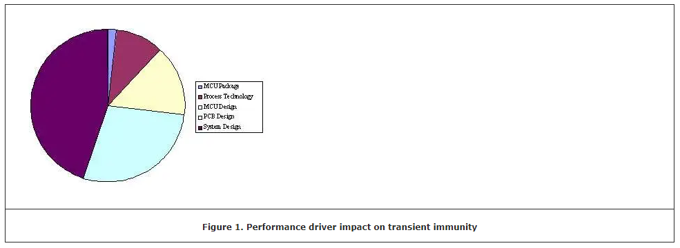
In addition to the process technology, MCU performance in the presence of an ESD or EFT event is affected by the design of the IC and its package, the design of the printed circuit board (PCB), the software running on the MCU, the design of the system, and the characteristics of the ESD or EFT waveform when it reaches the MCU.
除了工艺技术之外,IC及其封装设计、印刷电路板(PCB)设计、MCU上运行的软件、系统设计以及ESD或EFT波形到达MCU时的特性,都会影响MCU受到ESD或EFT干扰时的表现。
The relative impact of each performance driver (where to focus effort for maximum effect) is shown in the pie chart in Figure 1, below.
下面图1中的饼状图显示了每个驱动因素的相对影响(集中影响其最大的效果)。
Several facets of IC design other than physical gate length can affect MCU performance during transients.
除了物理栅极长度之外,IC设计的几个方面也会影响MCU的瞬态性能。
These include the composition of ESD suppression devices on input/output (I/O) pins and the layout of I/O pin structures.
其中包括输入/输出(I/O)引脚上ESD抑制器件的组成以及I/O引脚结构的布局。
ESD devices range from simple diodes to complex active filters.
ESD器件的范围从简单的二极管到复杂的有源滤波器。
Power supply rejection is accomplished through internal capacitance and careful routing on the die.
电源抑制是通过内部电容和芯片上的细致布线来实现的。
Physical separation of pin inputs from active circuitry is a proven method to reduce transient effects but at a greater cost penalty due to die size impact.
引脚输入与有源电路的物理隔离是一种行之有效的降低瞬态效应的方法,但由于芯片尺寸的影响,成本会更高。
The choice of MCU package can also affect immunity performance.
MCU封装的选择也会影响抗扰度性能。
The package type can have a great influence on PCB layout and composition.
封装类型对PCB布局和结构有很大影响。
Surface-mount MCUs generally have smaller footprints than through-hole packages.
表面贴装MCU的尺寸通常小于通孔封装。
This can reduce overall PCB dimensions and increase routing density, but it can also provide more space to implement board-level suppression techniques.
这可以减小PCB的整体尺寸,提高布线密度,但也可以提供更多空间来实施板级抑制技术。
Areas of MCU Vulnerability MCU脆弱的地方
Considering that most MCUs are specified and designed to generate and respond to signals with rise times comparable to ESD and EFT events, vulnerability to these events should be expected.
考虑到大多数MCU是被指定和设计于生成和响应信号,而这些信号的上升时间是和ESD和EFT相当的,我们应该预料到这些情况的薄弱点。
Areas of MCU's typically vulnerable to ESD and EFT stresses include:
MCU通常易受ESD和EFT压力影响的地方包括:
Power and ground pins 电源和接地引脚
Edge sensitive digital inputs 数字输入的边沿干扰
High frequency digital inputs 高频数字输入
Analog inputs 模拟输入
Clock (oscillator) pins 时钟(晶振)引脚
Substrate injection 基板内部干扰
General purpose I/O (GPIO) with multiplexed pin functions 引脚多路复用功能的通用I/O (GPIO)
ESD protection circuitry ESD保护电路
Some MCUs have multiple power and ground pins to isolate high speed digital functions from low speed or noisy analog functions.
一些MCU有多个电源和接地引脚,用来隔离高速数字功能和低速或有噪声的模拟功能。
These supply pins should be filtered appropriately to prevent disturbances in one area from affecting another.
这些电源引脚应经过适当滤波,以防止一个区域的干扰影响到另一个区域。
Low cost MCUs may only have a single set of power and ground pins, which makes isolation difficult, and makes filtering more important.
低成本的MCU可能只有一组电源和接地引脚,(信号)隔离就变得困难,所以电源滤波就更加重要了。
It is easy to understand that a transient that gets propagated to a supply line can also disrupt internal circuitry that has no direct route to the pin that was disturbed.
很容易理解,传播到供电线的瞬态干扰也可以破坏内部电路,而此时内部电路是没有直接连接到被干扰的引脚。(这说明,干扰可以通过影响电源线间接地影响系统的工作)
Edge sensitive inputs are particularly vulnerable to transients.
输入的边沿信号特别容易受到瞬态干扰的影响。
These inputs are usually timer or external interrupt inputs.
这些输入通常是定时器或外部中断输入。
Even with external low pass filtering, a sufficiently large pulse can inject enough energy into the input area to disrupt MCU operation.
即使使用外部低通滤波器,一个大的脉冲也可以注入足够的能量到输入电路,从而扰乱MCU的操作。
Pulses that don't disrupt the MCU can still be seen as glitches by the MCU. (A software technique to filter out glitches is discussed later in this series ).
没有扰乱MCU工作的脉冲仍然可以被MCU视为故障。(本系列后面将讨论一种过滤故障的软件技术)。
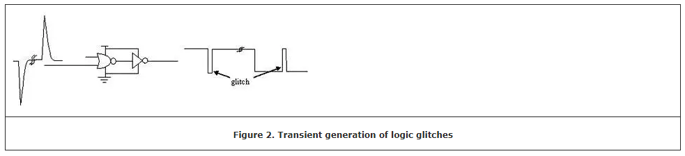
High speed digital inputs, such as clock and data inputs, are less likely to have and consequently can register transients as valid data pulses (see Figure 2, above) .
高速数字输入,如时钟和数据输入,不太可能有,因此可以将瞬态干扰调整为有效的数据脉冲(参见上图2)。
External isolation techniques are necessary to eliminate this vulnerability.
为消除这些干扰,必需做好外部的隔离。
Analog inputs are generally lower impedance than digital inputs and can suffer physical damage if not protected during ESD and EFT transients.
模拟输入通常比数字输入阻抗低,如果在ESD和EFT瞬态过程中没有保护,可能会遭受物理损坏。
However, on most MCUs the analog inputs are multiplexed with general purpose I/O pins and have a small sampling window in which the lower input impedance is active.
然而,在大多数MCU上,模拟输入与通用I/O引脚进行多路复用,并且有一个小的采样窗口,这时使用了较低的输入阻抗。
A transient appearing in an analog input pin during an analog to digital conversion will result in distorted data due to the signal disruption.
在模拟到数字转换过程中,模拟输入引脚中出现的瞬态干扰,会扰乱信号而导致数据失真。
Effective software filtering techniques exist to mitigate this vulnerability.
设计有效的软件滤波技术可以减轻此干扰。
Most MCUs have a built-in oscillator amplifier so that an external crystal or resonator is all that is needed to ensure a stable high frequency system clock.
大多数MCU都有一个内置的振荡器放大器,这样就需要一个外部晶体或谐振器来确保稳定的高频系统时钟。
The oscillator pins can pass noise pulses as valid clock edges and are considered to be the most vulnerable inputs to the system.
振荡器引脚可以通过带有噪声的脉冲作为有效的时钟边沿,被认为是系统最脆弱的输入点。
Appropriate PCB layout is the preferred method to eliminate this risk.
适当的PCB布局是消除这种风险的首选方法。
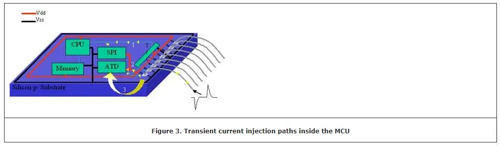
As shown in Figure 3 above , transients can travel from the point of entry and affect circuits via several paths.
如图3所示,瞬态干扰可以从输入点通过多条路径影响电路。
System input signals that exceed the power rails of the MCU will inject current into the I/O pin structure as soon as the signal level exceeds the ESD protection diode's forward voltage.
那些超过MCU电源轨道的输入到系统的信号,一旦信号电平超过ESD保护二极管的正向电压,就会向I/O引脚结构注入电流。
The I/O pin structure and on chip ESD protection network can dissipate small amounts of injected energy.
I/O引脚的结构和片上ESD保护网络可以耗散少量的注入能量。
However, if the injected current is greater than the local circuit can handle, this excessive current can find alternate paths through the supply rails or substrate to disrupt other circuitry.
但是,如果注入的电流大于了本地电路所能处理的(电流),这种过量的电流会找备用路径流过——这些电流就流过供应电源轨道或基板,干扰了其他电路。
Current injection is generally minimized by using series resistors.
最小化注入电流影响通常通过使用串联电阻解决。
General purpose MCUs have I/O ports that can have more that one function multiplexed on a single pin.
通用MCU具有I/O端口,可以在单个引脚上多路复用多个功能。
An electrical disturbance that causes enough energy to disrupt digital logic can also affect the control circuitry that selects the pin function.
那些带有能够扰乱数字逻辑的能量的电气干扰,也会影响到选择引脚功能的控制电路。
The resulting fault could change the pin state, the pin directionality, or the pin function.
由此产生的故障可能会改变引脚状态、引脚方向或引脚功能。
Vulnerability is particularly troublesome for general purpose MCUs that are designed to meet the needs of many applications.
对于被设计来满足多种应用需求的通用MCU来说,易受干扰是尤其麻烦的。
For these MCUs, it is impractical or impossible to harden all vulnerable areas without adversely affecting functional performance in at least some applications.
对于这些MCU来说,至少在某些应用中,在不影响功能性能的情况下,加固所有易受干扰的区域是不切实际或不可能的。
Application-specific MCUs can be hardened with greater success, but some vulnerability will continue to exist if the operational frequency or bandwidth of the MCU overlaps the bandwidth of the ESD and EFT signals.
特定应用的MCU可以更好的被加强(防干扰的能力),但是,如果MCU的工作频率或带宽与ESD和EFT信号的带宽重叠,那么一些干扰将继续存在。
MCU Immunity Performance Classification 单片机免疫性能分类
The immunity performance for integrated circuits is typically classified into one of four categories as specified in and shown in Table 1 below .
集成电路的抗扰性能通常分为中规定的四类之一,并在下面的表1中所示。
The classification applied is determined by the performance of the integrated circuit in the presence of the disturbance signal (i.e the ESD or EFT waveform).
该分类是由集成电路在干扰信号(即ESD或EFT波形)存在时的性能表现决定的。
This performance is dependent on the type of integrated circuit and its functional and parametric operation as documented in its data sheet.
这种性能取决于集成电路的类型及其数据表中的功能和参数。
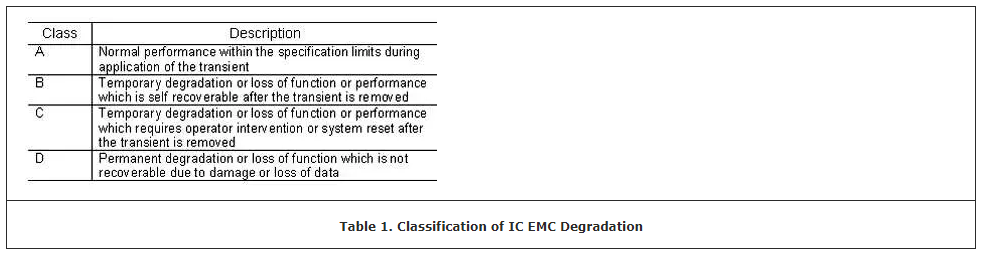
Class A performance is the most desirable and is often required for safety-critical applications.
A类性能是最理想的,通常应用于关键安全领域。
Of course, this level of performance is difficult to ensure without taking proper steps in the design of the application.
当然,如果在应用程序的设计中不采取适当的步骤,就很难保证这种级别的性能。
This is because any transient appearing at a pin that can be processed by the input circuitry has the potential for being interpreted as data and corrupting program execution.
这是因为在输入电路的引脚上出现的任何瞬态干扰,被处理后都有可能被理解为数据,并影响程序执行。
Class B performance is considered acceptable for most applications where the main requirement is for no user intervention to recover normal performance.
B类性能被认为是大多数应用程序可以接受的,主要应用是免除用户去恢复到正常性能。
Class C performance can be acceptable for particular applications where operator intervention is not an issue, or where an external watchdog or supervisory circuit is used.
C类性能可用于操作员可以进行干预的,或使用外部看门狗或监控电路的特定应用。
Class D performance is not acceptable.
D类性能不能接受的。
MCU Failure Modes MCU故障模式
For MCUs, performance degradation can take many forms. Common forms oftemporary degradation include but are not limited to reset, latch-up,memory corruption, and code runaway.
对于微控制器来说,性能下降可以有多种形式。常见的临时降级形式包括但不限于重置、锁存、内存损坏和代码失控。
MCUs with internal reset circuits can generally resume operation without operator involvement if the fault is an unexpected reset or code runaway that is caught by a watchdog timer.
如果故障是由看门狗定时器捕捉到的意外复位或代码失控,带有内部复位电路的MCU,通常可以在没有操作员干预的情况下恢复正常工作。
Recovery from latch-up and volatile memory (RAM, DRAM, etc.) corruption requires cycling the power to the system.
从锁存和易失性内存(RAM、DRAM等)损坏中恢复,需要对系统重启供电。
Non-volatile memory (FLASH, EEPROM, ROM, etc.) corruption requires a more extensive process of re-programming the system, which can be viewed as a temporary MCU degradation if the system can be re-worked, or as a permanent degradation if it cannot be re-worked.
非易失性存储器(FLASH、EEPROM、ROM等)损坏需要对系统重新编程的更复杂的过程,如果系统可以重新工作,则可以将其视为暂时的MCU损坏,如果不能重新工作,则将其视为永久损坏。
Permanent degradation can include increased leakage current on I/O pins which can affect analog measurements, input impedances, and output drive strength.
永久损坏可能包括I/O引脚上的泄漏电流的增加,这会影响模拟的测量、输入阻抗和输出驱动强度。
With increased leakage current, the electronic system may still operate within specification for a while, but it may ultimately fail due to damage from the transient stress.
随着漏电流的增加,电子系统仍可在规范范围内工作一段时间,但最终可能因瞬态干扰的压力而损坏。
Another type of permanent degradation found in transient environments is blown pins due to an electrical overstress.
在瞬态干扰环境中发现的另一种永久性损坏是由于过压引起的引脚爆炸。
Impact of MCU Design Trends MCU设计趋势的影响
The MCU design trend that particularly impacts transient immunity performance is the drive to continually reduce the minimum gate length of individual field effect transistors (FETs), making them smaller and faster.
特别是影响到瞬态抗扰度性能的MCU设计的趋势,是驱使着不断地减小单个场效应晶体管(FET)的最小栅极长度,使它们更小、更快。
This trend is the result of market pressure on semiconductor manufacturers to reduce the cost of their products by making die sizes smaller.
这一趋势是市场竞争的结果,半导体制造商通过缩小产品的尺寸来降低成本。
The result is that maintaining the immunity performance of MCUs in the face of process technology advances is becoming increasingly difficult.
结果是,面对工艺技术的进步,保持MCU的抗扰性能变得越来越困难。
When coupled with continuing cost reductions by OEMs at the application or system level, the immunity problem becomes severe.
当再加上原始设备制造商在应用程序或系统层面上不断降低成本,免疫问题就会变得非常严重。
MCU designers are challenged to develop better methods to dissipate the energy injected during a transient event.
MCU设计人员面临的挑战是找到更好的方法来耗散瞬态干扰注入的能量。
While they would appreciate more area in which to include transient suppression circuits, this is generally not allowed in order to keep the die size and cost to a minimum.
虽然他们希望在更多的区域包含瞬态抑制电路,但为了使尺寸和成本最小化,这通常是不允许的。
Some of the remaining options available to the designer include modifying semiconductor attributes (doping and materials) and changing the vertical structure of the I/O pin.
对于设计师可选的一些剩余选项,包括修改半导体属性(掺杂和更换材料)和改变I/O引脚的垂直结构。
Next in Part 2: Hardware Techniques- The basic circuit building blocks 第二部分:硬件技术-基本电路构建块
Ross Carlton has specialized in all aspects of electromagnetic compatibility (EMC) since his graduation from Texas A&M University with a Bachelor of Science in Electrical Engineering in 1985. He has been with for the last eight years where he has led the EMC design, test and support of Freescale's 8, 16, and 32-bit microcontroller products. In addition,Ross represents the U.S. as a Technical Expert to Subcommittee 47Aon integrated circuits where he is the project leader for IEC 61967-2,IEC 61967-3 and IEC 62132-2. He is currently involved in developing transient immunity test methodologies for standardization.
The author would like to thank Greg Racino and John Suchyta, 8-Bit Applications Engineer at Freescale Semiconductor for their inputs and guidance. Their contributions were critical to ensuring consistent and correct guidance.
References:
1. Ross Carlton, Greg Racino,John Suchyta, Improving the Transient Immunity Performance of Microcontroller-based applications. .
2. IEC 61000-4-2,Electromagnetic compatibility (EMC) – Part 4-2: Testing and measurement techniques – Electrostatic discharge immunity test, , 2001.
3. IEC 61000-4-4,Electromagnetic Compatibility (EMC) – Part 4-4: Testing and measurement techniques – Electrical fast transient/burst immunity test,International Electrotechnical Commission, 2001.
4. Ronald B. Standler,Protection of Electronic Circuits from Overvoltages, John Wiley &Sons, 1989, pp. 265-283.
5. Ken Kundert, “PowerSupply Noise Reduction”, , 2004.
6. Larry D. Smith,”Decoupling Capacitor Calculations for CMOS Circuits”, , Monterey CA,November 1994, Pages 101-105.
7. Ronald B. Standler,Protection of Electronic Circuits from Overvoltages, John Wiley &Sons, 1989.
8. Clayton Paul, , Wiley & Sons, 1992.
9. Bernard Keiser,Principles of Electromagnetic Compatibility, Artech House, 1987.
10. T.C. Lun, “Designing for Board Level Electromagnetic Compatibility”,

 浙公网安备 33010602011771号