FedericoFaggin介绍
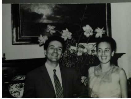
Federico Faggin was born in Vicenza. (1, december 1941),Federico’s parents, Emma and Giuseppe, with Giorgio (left) and Federico, at Isola Vicentina.
如果您要查找世界上第一个商用微处理器(intel 4004)并仔细查看芯片内部电路,您可能会发现在一个角落有一个小小的签名,即缩写FF-Frederico Faggin。
费德里科·法金(FedericoFaggin)直接或间接创立和领导的几家新兴公司,从19岁起就赋予了许多最先进的产品和技术以生命。
1961年,他在奥利维蒂(Olivetti)共同设计并建造了实验性晶体管电子计算机。在飞兆半导体公司,他开发了几种用于集成电路制造的工艺技术,其中之一是MOS硅栅技术(1968),该技术已在全球范围内采用,并一直沿用至今。飞兆半导体3708,是世界上第一个带有SGT的集成电路。
Faggin设计了世界上第一个商用微处理器Intel 4004(1971),开发了设计方法并指导了所有早期Intel微处理器的设计。其中杰出的是intel的8008(1972)和8080(1974)。
1974年,Faggin创立并领导了他的第一家公司Zilog,Inc.,该公司完全致力于新兴的微处理器和微控制器市场。Zilog Z80微处理器(1976年)和Z8微控制器(1978年)在2014年仍处于批量生产。他还为多家公司开发了数十个存储芯片和其他集成电路。
Faggin创立并指导了CygnetTechnologies,Inc.(1982);该公司于1984年推出了一种用于语音,数据和电子邮件的开创性个人通信产品。他创立并指导了Synaptics Inc.(1986);该公司开发了用于进行模式识别的人工神经网络芯片。今天,Synaptics成为人机界面解决方案的领导者,率先开发了Touchpad(1994)和Touchscreen(1999),它们彻底改变了我们与移动设备交互的方式。在2003年至2008年期间,Faggin担任Synaptics董事长兼Foveon,Inc.首席执行官,该公司是用于移动设备的高级图像感应器和数码相机的开发商。
Faggin目前是Federico和Elvia Faggin基金会的主席,该基金会是致力于意识科学研究的非营利组织,长期以来的兴趣已经变成了一项充满激情的全职活动。
费德里科·法金(FedericoFaggin)在美国,欧洲和日本获得了许多奖项。其中杰出的奖项包括马可尼奖(1988),京都先进技术奖(1997),欧洲专利组织的终身成就奖(2006)和2009年巴拉克·奥巴马(BarackObama)总统颁发的国家技术与创新奖章。Faggin于1996年因共同发明微处理器而入选国家发明家名人堂,他还获得了计算机科学和电子工程学的许多荣誉学位,包括亚美尼亚理工大学的电子工程学博士学位,以及查普曼大学(ChapmanUniversity)理学博士学位。
Faggin在Fairchild期间开发了MOS硅栅极技术,该技术可实现自对准栅极,这是微处理器中所有现代集成电路的技术基石。Faggin在intel与Fackin以及Marcian Hoff和Stan Mazor一起开发了世界上第一个商用微处理器Intel 4004。
以下来自 http://www.intel4004.com/index.htm
1.Federico Faggin signed the 4004 because: 费德里科·法金设计4004的原因是:
- He was the leader of the design/development project of the first microprocessor, and brought it to its successful conclusion.
- 他领导了第一个微处理的项目即4004芯片的开发,并且圆满地完成了这个项目
- Faggin did the detailed design work (logic design, circuit design, chip layout, tester design and test program development) with help from Masatoshi Shima, a Busicom software and logic designer without any previous chip design experience.
- 法金在没有任何芯片设计经验的Busicom软件和逻辑设计师Masatoshi Shima的帮助下,详细的设计工作包括了逻辑设计,电路设计,芯片布局,测试和测试程序开发等
- Busicom presented to Faggin the engineering prototype of their calculator with the first 4004. Faggin in 1996 donated it to the Computer History Museum in Silicon Valley.
Busicom 公司把整个工程交给了法金来实施,法金与1996年把这个项目捐赠给了在Silicon Valley的计算机博物馆
博物馆主页:http://www.computerhistory.org/
- He was the original developer of the Silicon Gate Technology, at Fairchild Semiconductor in 1968, the first commercial self-aligned gate process, and the designer of the world's first commercial integrated circuit using the silicon gate technology: the Fairchild 3708. This semiconductor technology was copied by Intel and made into its core manufacturing technology, enabling the early realization of high-performance memories and the microprocessor.
他是硅栅技术的最初开发者,1968年在飞兆半导体公司
许多电脑史学家都认为,要想了解美国硅谷的发展史,就必须了解早期的仙童半导体公司(Fairchild Semiconductor),也译作飞兆半导体公司。这家公司,曾经是世界上最大、最富创新精神和最令人振奋的半导体生产企业,为硅谷的成长奠定了坚实的基础 - 第一个商业化的自对准栅极工艺,以及世界上第一个使用硅栅极技术的商业集成电路的设计者:Fairchild 3708。这项半导体技术被英特尔复制并制成其核心制造技术,使高性能存储器和微处理器得以早期实现
- Faggin made two other key inventions at Fairchild: the Buried Contact and the Bootstrap Load. At Intel he applied these innovations to build the first microprocessor. They were essential in making the 4004 a reality with the technology available in 1970. Faggin also created the basic Methodology for Random Logic Design using silicon gate technology. This methodology did not exist at Intel or anywhere else until he developed it in 1970. It set the style of design used for all early generations of microprocessors at Intel.
- 法金在飞兆的两个其他的关键发明是网络埋入式的电极和Bootstrap Load
- Bootstrap Load是一种电路技术参考: http://www.intel4004.com/btstrp.htm
- He also created a very innovative layout and invented many special circuits, for example: a static MOS shift register, a new type of counter and a new automatic power-on reset circuit (US patent 3,753,011).
他还创造了一个非常创新的布局,并发明了许多特殊电路,例如:静态金属氧化物半导体移位存储器
- He demostrated that the 4004 could be used for applications other than calculators and vigorously campaigned inside Intel to make the 4004 available to the general market.
他演示了4004可以用于计算器以外的应用程序,并在英特尔内部大力宣传将4004推向普通市场
- Two patents cover Intel's MCS-4: patent no. 3,821,715, Memory System for a Multi-Chip Digital Computer, in the names of Ted Hoff, Stan Mazor and Federico Faggin (filed January 1973, granted June 28, 1974); and patent no. 3,753,011, power supply settable, bi-stable circuit, in the name of Federico Faggin (filed March 13, 1972, granted August 14, 1973).
- 两项专利涉及英特尔的MCS-4:专利号3821715,多芯片数字计算机的存储系统,以泰德·霍夫、斯坦·马佐尔和费德里科·法金的名义(1973年1月提交,1974年6月28日授予);专利号3753011,电源可设置,双稳态电路,以Federico Faggin的名义(1972年3月13日提交,1973年8月14日授予)
After designing the 4004, Federico Faggin intensely promoted within Intel the broad commercialization of microprocessors, which at the outset were only custom products, to the general market. He was in charge of the design and development of all Intel's early microprocessors: the 4004, 8008, 4040 and 8080.
在设计了4004之后,费德里科·法金在intel内部大力推动微处理器的广泛商业化,从一开始,微处理器只是定制产品,进入普通市场。他负责英特尔早期所有微处理器的设计和开发:4004、8008、4040和8080。
He conceived and defined the architectures of the 4040 and of the 8080, and supervised their design and development. He presented his architectural proposal for the 8080 to management in early 1972, urging his boss to start the project in earnest, but management wanted to ascertain the market reaction to the recent introduction of the 4004 and 8008 before committing additional resources. Nine months of competitive advantage were thus lost due to this indecision. Intel was then a semiconductor memory company and microprocessors were not a priority.
他构思并定义了4040和8080的体系结构,并监督了它们的设计和开发。1972年初,他向管理层提交了8080的建筑方案,敦促他的老板认真启动该项目,但管理层希望在投入额外资源之前确定市场对最近推出的4004和8008的反应。由于这种犹豫不决,九个月的竞争优势因此丧失。英特尔当时是一家半导体存储器公司,微处理器不是优先考虑的问题
The silicon gate design methodology and the novel layouts created by Faggin for the 4004 provided a source of techniques and implementation examples that were subsequently used at Intel and other companies for the design of complex random logic chips.
|
2.Federico Faggin 2001年11月15日在圣何塞的微处理器论坛演讲稿
Federico Faggin
Invited paper presented at the Microprocessor Forum San Jose, CA, October 15, 2001
It is a pleasure to be here tonight to share with you my microprocessor adventure. Looking back, it seems to me that all my prior experience prepared me for the design of the first microprocessor. When I was 19 I co-designed and built a small digital computer at Olivetti in Italy. I say small, but actually it was the size of a cabinet. It was 1961. Then, after I studied solid-state physics at the University of Padua, I became the MOS group leader of SGS-Fairchild in Italy - what is now ST Microelectronics - where I developed their first MOS process technology and designed a couple of integrated circuits. I then came to the US in February of 1968, to work for Fairchild Semiconductor in their R&D Laboratory in Palo Alto. At Fairchild, following some preliminary work done by Tom Klein, I developed the silicon gate technology, the world's first manufacturing process for the fabrication of P-channel, self-aligned-gate MOS integrated circuits. I also designed the first commercial integrated circuit with self-aligned gates (the Fairchild 3708). With silicon gate it became possible to make integrated circuits 3 to 5 times faster, 50% to 100% denser, more reliable, and with much lower leakage current than with aluminum gate technology, the only other MOS technology available. Intel, founded in 1968 by mostly Fairchild employees -- among them was my boss, Les Vadasz ad Andy Grove, both familiar with my work -- adopted the new silicon gate technology.
In April 1969, Busicom, a Japanese calculator manufacturer, having heard that Intel had the best manufacturing technology in the industry, visited them with a very demanding custom job. The Busicom design consisted of a programmable decimal computer with ROM-based macro-instructions and shift-register data memory, partitioned into seven different chips. The chips were to be used for a family of products, starting with a desktop printing calculator, at the low end, and ending with cash registers and billing machines at the high-end. Dr. Ted Hoff, who at that time was the manager of the application research department of Intel, was called in to evaluate the opportunity. Ted was familiar with computers, having worked with IBM 1620 and 1130 at Stanford University. Looking at the Busicom design he was surprised by its complexity. He was also concerned with the magnitude of the task: Intel didn't have enough engineers to do all of that work. With the encouragement of Bob Noyce, Ted started considering alternative, simpler designs that might use the three-transistor RAM cells instead of the six-transistors shift register cells. He was naturally led to consider the design of a general-purpose computer that might be programmed to perform calculator functions.
This initial work occurred in July and August of 1969. In September Stan Mazor, coming from Fairchild, joined Hoff's group. With one more person on the team the work started accelerating. Working with the Busicom engineers, sometimes in a mildly adversarial climate, the architecture of the CPU and three other companion chips took shape to the point that Busicom people started feeling comfortable with it. In October 1969 the Busicom management chose the Intel architecture over theirs. Masatoshi Shima, the principal designer of Busicom, remained at Intel until December 1969 to program some of the critical routines with the newly minted instruction set, to verify that the job could be indeed done. Intel was to start immediately the logic and circuit design of the four chips, slated for sampling seven months later, according to a very optimistic development schedule prepared by Les Vadasz.
In April 1970 I joined Intel as the project leader of the Busicom chip set. Les Vadasz, my new boss, had been rather secretive with me in the job interview. I only knew that I had to design a set of four chips with random logic. The first day of work, I was introduced to Stan Mazor who gave me the general specification of the chip set - essentially a few block diagrams and the instruction set. He also told me that the next day Shima would arrive from Japan. We both went to greet Shima at the San Francisco airport and as soon as Shima settled in my office he asked me to show him the progress made. He was expecting to check the logic and circuit design of the chips, just as scheduled, but no work had been done since his departure from Intel in December. I gave him the material I had just received from Stan, and he immediately said that he already had that. "This is just idea" he said, "where is design"! Shima was furious because his product schedule was irreparably compromised.
It took me the best of one week to calm him down and make him understand that I had just joined Intel and that I could not possibly have done the design in one day. I finally succeeded in convincing him that we were both in the same boat, that if he stopped bitching and started helping, we might actually get the job done sooner. From that point on I was on my own. I was the leader of the project, but I had no staff, Hoff and Mazor were no longer involved with the project, and my boss Vadasz, the manager of the MOS design department, was 100% preoccupied with the 1kbit DRAM - the 1103, the future of Intel.
A few days after Shima's arrival, I prepared a new project schedule, more realistic than the one he had been given. I promised that it would take nine months to get to samples, knowing that I was still very optimistic. So now I was saying that the project would take nine months instead of seven, and we were already five months late. There were a number of agitated calls in Japanese across the Pacific. The project actually got close to be cancelled, but eventually Busicom management decided to continue with it and asked Shima to stay on to help me for six months. This was definitely not a good start.
My first task was to develop the design methodology for random logic circuits using silicon gate technology. This work had never been done before. Intel had used silicon gate technology only for memory chips and had no experience in random logic. There were two critical innovations of mine that made the CPU possible: the use of buried contacts and the use of bootstrap loads. The first innovation allowed to make direct contact between poly-silicon and junctions without having to use metal. Used properly, it provided a second layer of interconnections, reaching the gate density necessary for a cost-effective chip. The other innovation was the bootstrap load -- a circuit trick widely used with metal gate MOS circuits - but considered unfeasible with silicon gate technology without using an additional masking layer. Bootstrap loads allowed the use of dynamic nodes without sacrificing power and speed or having to use a lot more transistors for the job. There was no other viable technique with a good speed-power product, except for four-phase logic, which had its own major drawbacks. I figured out how to make bootstrap loads without an additional masking step, paving the way for an efficient design. Unquestionably, the speed and the circuit density enabled by the silicon gate technology were decisive factors in the birth of the microprocessor in 1971 instead of a few years later. I also devised a method of random logic design that combined logic and circuit building blocks -- including some novel circuits -- with layout information, to make the design faster and less error prone. I then proceeded with the logic and circuit design of the 4001 first. The 4001 was a 2 kbit metal-mask programmable ROM with a 4-bit mask-programmable input/output port. Next came the 4003 design, the simplest of the chips, a 10-bit serial-in, parallel-out and serial-out static shift register. Then the 4002, a 320-bit dynamic RAM with a 4-bit output port and finally the 4004, the 4-bit CPU. During this time Shima, under my direction, gave me great help in a variety of technical chores. The rest of the team consisted of three layout draftsmen and one electronics technician.
The project was like fast-tracking four buildings, with design and construction going on simultaneously. All was done by hand: the circuit schematics used large blue-line sheets, the composite layout was done with colored pencils over mylar at 500X. Then came the rubylith cutting, done by hand for each layer with the help of a precision cutting table. We also had to design and build the tester and the test programs for both chip characterization and production testing. I worked 70 to 80-hour weeks until the project was completed. I was lucky that Marzia - our first baby, just born in March 1970 - was channeling all of my wife Elvia's energy. She also spent the three summer months with her family in Italy, leaving me guiltless to work around the clock.
The 4001 was the first chip to come out of manufacturing, in October 1970. I was nervous because I had never designed a chip of that complexity before. Fortunately the chip worked perfectly giving me confidence that the rest of the project was sound. Shima, a bit more relaxed by the good news, went back to Japan at that time. In November, the 4003 and then the 4002 were also manufactured and they both worked. And finally the big day came. It was the end of December 1970. If the 4004 worked I would have met the impossible nine-months schedule. Fortunately, by the time I got the 4004 wafers, everybody had left the laboratory so no one could witness my trembling hands. I loaded the first 2'' wafer into the prober and lowered the probes onto the first die -- an oscilloscope was also connected to some of the critical signals. I pushed the start-test button and… nothing. I mean nothing, not even a wiggle anywhere in the scope. I told myself, it's a bad die, let me try another one: same story, there was nothing moving. I changed wafer and I repeated the process. Same result. By now I was profusely sweating, thinking: How could I have screwed up so bad? I continued to test more dies and more wafers. No life. After 20 minutes of agony I finally decided to take a look under the microscope; something must be wrong! It didn't take long to find out that the buried-layer masking step was left out of the process. No wonder there was no life! Most of the gates were floating! I made peace with myself, simultaneously with getting mad at the manufacturing guys for this screwup that cost me a three-weeks delay. Now the project was definitely going to be late.
I finally received new 4004's in January 1971. I spent most of the night alone, testing it. Everything that I tested worked perfectly and by 4:00 am I went home in a state of elation, sharing my excitement with Elvia, who was waiting for me. That was the night the 4004 was born. In the following days I found a few minor problems that I soon corrected, but the calculator project could now continue with confidence at Busicom. I sent Busicom fully working samples in late March - the calculator kit included one 4004, two 4002's, three 4003's and four 4001's containing the calculator firmware -- and by April, word came that the calculator worked perfectly. We could now start production.
Soon after joining Intel I found out that the 4000 family was an exclusive design for Busicom. I was disappointed because I wanted to design a standard product. I also found out that there was another single-chip CPU design going on, the 1201. The 1201 was casting in silicon the microcomputer architecture designed by Datapoint for their intelligent terminal. It was another exclusive custom design and Hal Feeney had responsibility for the project. I actually thought that the 1201 would become the world's first microprocessor, since the project had already started and Hal had only one chip to design while I had four -- the 4004 being the last to be designed. I resigned to that fact and soon I was too busy to worry about it. But then the 1201 project languished and Hal was asked to design a new memory chip. I inherited the mothballed project in January 1971, with Hal completing the project, working under my direction.
By that time I also started urging management to market the microprocessors broadly. I was getting the message by everybody, including Hoff and Mazor, that the 1201 may be OK but that the 4004 was good mainly for calculators, and that it would be difficult to get Busicom to relinquish its exclusivity. But I wanted to see the 4004 in the market! I argued that the 4004 could be used effectively in many control applications and to prove the point I used it as the controller of a production tester I was designing. I used the success of that project to convincingly show management that anybody else could use it as well. Some time later I found out from Shima that Busicom was in financial difficulty. I then suggested to Bob Noyce to renegotiate the contract trading the exclusivity clause for a price concession. The strategy worked and by November 1971 the 4000 family was announced to the world with a new name: MCS-4 - microcomputer system 4-bit. By April 1972, the 1201 with the market name 8008 was also announced. It was the world's first 8-bit microprocessor, the core member of the MCS-8 family.
Hoff, Feeney, Mazor and I were all involved helping the early marketing efforts of the newly formed microcomputer marketing department under the direction of Hank Smith. I vividly remember a trip to Europe to visit customers with Hank. This trip occurred in the late summer of 1971, a few months before the MCS-4 introduction. I found out that the more computer literate the customer, the more resistant he was to consider using the microprocessor. The worst meeting was at Nixdorf Computer where they nearly ridiculed us for the poor architecture of our machines. Some of their criticism was valid, to be sure, but the level of hostility was only justified by the more or less conscious awareness that a turf war was beginning with the semiconductor guys. Well, we know who is left standing 30 years later!
The first applications were primarily driven by non-computer customers that had a problem to solve - not a philosophical debate. For many low-volume applications, the task of designing the hardware using conventional components was too daunting, costly and inflexible. With the microprocessor, the solution was a much more flexible software program. Gas pump controllers, traffic controllers, automatic blood analyzers, in addition to all forms of calculating machines were the first applications of the MCS-4. Intelligent terminals and programmable microcomputers were the first applications of the 8008. It turned out that the MCS-4 became the archetype of the microcontroller business, while the 8008 became the archetype of the microprocessor business.
During my 1971 trip to Europe, listening to customer inputs, I realized that we could do better. In the next few months I developed the basic architecture of what was to become the 8080. I described it in a memo to Vadasz in April 1972, urging him to let me start the project immediately. But Intel was in no hurry, they wanted to see how the newly introduced products were doing in the market before committing more resources. The project only started in November 1972 and our market lead shrank to six months to the Motorola's 6800. Nonetheless, the 8080 was highly successful.
Intel in those days was a memory company. Microprocessors were important only insofar as they helped sell memory chips. I had always felt a second-class citizen at Intel. I believed in microprocessors so I decided to start my own company, completely dedicated to the new business. I made that decision in the summer of 1974, a few months after the market introduction of the 8080. I finally left Intel in October 1974 and with Ralph Ungermann, one of the managers reporting to me, I started Zilog.
I conceived the Z80 microprocessor family in December 1974. It was a Saturday. I had been struggling for some time to figure out our first product. Then it came in a flash: I said aloud, Super-80! And with that exclamation, the basic architecture of the Z80 family came vividly into focus. I don't have enough time left to tell that story, except that the Z80 is one of the most successful microprocessors ever produced: it is still in high-volume production today, 25 years after its market debut.
With Zilog a new chapter of my life started: I changed from an R&D guy into an entrepreneur and CEO, activity that has continued until a couple of years ago. Over the last 25 years I started and was CEO of three start-up companies. Two years ago I decided that it was time to slow down a bit. I am now the Chairman of the Board of my last start-up, Synaptics. We produce human-to-computer interface products using neural networks and mixed-signal technology. I am also Chairman of the Board of IDT; board member of five other companies and an angel investor. For the first time in my life I have plenty of time to travel for pleasure, read about a variety of stimulating subjects and generally enjoy life. However, I am not ready to retire yet: if the right project were to come along, I know my creative juices would be flowing again.
自来: http://www.intel4004.com/speech.htm
其他资料
https://www.1000bit.it/storia/perso/faggin_interview.asp
http://www.fagginfoundation.org/biography/ Faggin的故事
https://newsroom.intel.com/editorials/computers-still-no-match-for-human-intelligence/#gs.w9zqny
https://www.computerhistory.org/siliconengine/microprocessor-integrates-cpu-function-onto-a-single-chip/