
Xilinx的V7系列FPGA中LC、CLB和Slice介绍(如何计算LC)
在Xilinx的FPGA的资源列表中常常有LC(logic cells)一项,LC代表什么呢,下面是Xilinx官方回答:
A "logic cell" is a marketing thing. It is an attempt to create a "unified" metric that can be used across different device families (and even different vendors) to compare sizes of devices even when the underlying architecture is different.
The "logic cell" is supposed to represent a 4-input LUT with no other functionality. In older Xilinx technologies (with 4-input LUTs) they used to use 1.25 as the multiplier to get from LUTs to Logic Cells, since the Xilinx slice also had the carry chain and wide MUX, which made it possible to do more than a simple 4-input LUT would be able to do.
In later technologies, which use the 6-input LUT, they use the multiplier 1.6.
Also remember there are two flip-flops per LUT...
So, the device has 2,443,200 flip-flops, which means 1,221,600 6-input LUTs. Multiply this by 1.6 and you get 1,945,560, which is the published "Logic Cells" number.
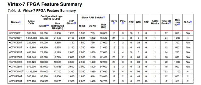
大概意思就是说“logic cells” 是 Xilinx 创造提出来的一个市场说法,可以用来衡量不同内部结构甚至不同厂商的FPGA芯片的资源情况。
"logic cells"代表的是一个没有其他任何功能的4输入LUT,在老一些的Xilinx的FPGA中,他们使用LUT的数目乘以1.2来计算LC的数目,因为一个LUT中还有一个进位链和MUX,这样可以使一个LC比淡出的4输入LUT实现更多功能。
在较新的FPGA中,Xilinx采用了6输入LUT,这时他们采用系数1.6。
另外请记住一个LUT对应这两个FF,也就是一个查找表对应两个寄存器。
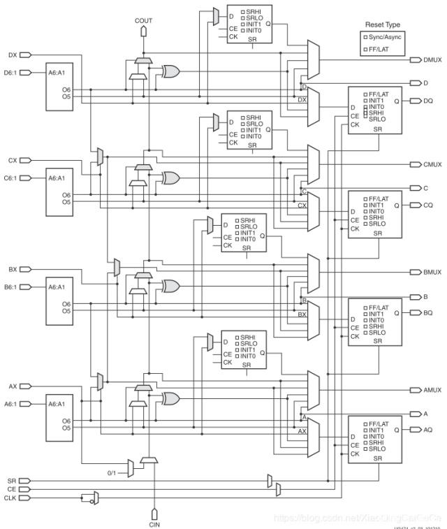
下面介绍slice:
Xilinx的官方文档在介绍FPGA的逻辑资源时通常是按照可配置逻辑块CLB(Configurable Logic Block)来介绍,把CLB作为FPGA里的最小逻辑单元。但是一个CLB是由2个slice构成,所以大家也常常把slice作为最小的逻辑单元。下面我们来介绍slice的组成:
V7系列FPGA的slice包含4个部分:
(1)LUT查找表,1个slice里包含4个6输入的查找表。
(2)存储单元,也就是常说的触发器,1个slice里包含8个触发器。每4个触发器为一组,可配置成D触发器或锁存器。
(3)多路复用器,也就是1位宽的数据选择器,数量非常多,足够使用。
(4)进位逻辑,它与本列的上下slice的进位逻辑相连,实现数据运算时的进位操作。
因此,许许多多的slice相结合,再加上全局时钟就能实现复杂的数字功能。另外,FPGA里的slice有2种,一种被称为sliceL,另一种被称为sliceM,有的CLB由2个sliceL构成,有的则是由1个sliceL和一个sliceM构成。SliceM除了基本功能外,可以实现RAM和移位寄存器的功能,这两种功能很有用,通过工具软件可以自动实现,不用咱们操心。

 浙公网安备 33010602011771号