SPI协议背景知识简介与FTDI的FT4232H配成USB to SPI(MPSSE)使用实例
MPSSE Application Example:
http://ftdichip.cn/Support/SoftwareExamples/MPSSE.htm
MPSSE: AN_129 FTDI USB To JTAG TAP Example
MPSS: AN_114 FTDI USB to SPI Example
MPSSE: AN_113 FTDI USB to I2C Example
MPSS: AN_114 FTDI USB to SPI Example
Acronyms and Abbreviations
| Terms | Description |
|---|---|
| MPSSE | Multi Purpose Synchronous Serial Engine |
| I2C | Inter-Integrated Circuit |
| JTAG | Joint Test Action Group |
| SPI | Serial Peripheral Interface |
| SPI Master | A SPI device that initiates and manages serial communication to all devices connected to its SPI bus. |
| SPI Slave | A SPI device that responds to commands sent to it by the SPI master. |
| MISO | Master In, Slave Out |
| MOSI | Master Out, Slave In |
| Serial EEPROM | A programmable memory chip that uses a bitwise serial interface such as I2C or SPI. |
| USB | Universal Serial bus |
FTDI MPSSE(Multi-Protocol Synchronous Serial Engine)
Using the MPSSE can simplify the synchronous serial protocol (USB to SPI, I2C, JTAG, etc.) design. This application note illustrates how to use the MPSSE of the FT2232H to interface with the SPI bus. The FT232H and FT4232H can also be used with the example in this document, though pin-out and port selection will need to match the respective part.
Users can use the example schematic (refer to Figure 3) and software code (section 3) to begin their design.
Note that software code listing is provided as an illustration only and not supported by FTDI.
1 Introduction
The FT2232H and FT4232H are the FTDI's first USB 2.0 Hi-Speed(480Mbits/s) USB to UART/FIFO ICs.
They have the capability of being configured in a variety of serial interfaces using the internal MPSSE (Multi-Protocol Synchronous Serial Engine). The FT2232H device has two independent ports, both of which can be configured using MPSSE while only Channel A and B of FT4232H can be configured using MPSSE.
1.1 Overview & Scope
This application note gives details of how to interface and configure the FT2232H to read and write data from a host PC to a serial EEPROM over the serial SPI interface bus. This note includes:
- Overview of SPI communications interface.
- Hardware example of a USB to a serial EEPROM SPI interface using the FT2232H.
- Code example in C++ showing how to configure the FT2232H in SPI mode.
- Oscilloscope plots showing example SPI read and write cycles.
1.2 Overview of SPI Interface
The SPI (Serial to Peripheral Interface) is a master/slave synchronous serial bus that consists of 4 signals.
Both command signals and data are sent across the interface.
The SPI master initiates all data transactions.
There is no fixed bit length in SPI.
Full duplex data transfers can be made up to 30Mbits/sec with the FT2232H.
A generic SPI system consists of the following signals and is illustrated in Figure 1.:
- SCLK(Serial Clock) from master to slave.
- CS(Chip Select) from master.
- MOSI(Serial Data Out, also called Master Out Slave In) from master.
- MISO(Serial Data In, also called Master In Slave Out) from slave.
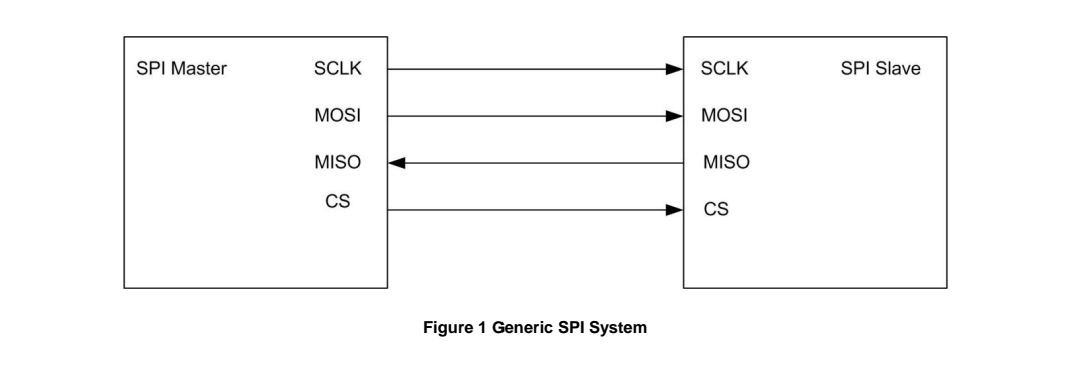
The FT2232H always acts as the SPI master. Multiple slave devices can be enabled by multiplexing the chip select line. As SPI data is shifted out of the master and in to a slave device, SPI data will also be shifted out from the slave and clocked in to the master.
Depending on which type of slave device is being
implemented, data can be shifted MSB first or LSB first.
Slave devices can have active low or active high chip select inputs.
This SPI device uses SPI Mode 0, with active low Chip Select.

In addition, the SPI interface has 4 unique modes of clock phase(CPHA) and clock polarity (CPOL), known as Mode 0, Mode 1, Mode 2 and Mode 3. Table 1 summarizes these modes:
| Mode | CPOL | CPHA |
|---|---|---|
| 0 | 0 | 0 |
| 1 | 0 | 1 |
| 2 | 1 | 0 |
| 3 | 1 | 1 |
Table 1 Clock Phase/Polarity Modes
For CPOL = 0, the base (inactive) level of SCLK is 0. In this mode:
- When CPHA = 0, data will be read in on the rising edge of SCLK, and data will be clocked out on the falling edge of SCLK.
- When CPHA = 1, data will be read in on the falling edge of SCLK, and data will be clocked out on the rising edge of SCLK.
For CPOL = 1, the base (inactive) level of SCLK is 1. In this mode:
- When CPHA = 0, data will be read in on the falling edge of SCLK, and data will be clocked out on the rising edge of SCLK.
- When CPHA = 1, data will be read in on the rising edge of SCLK, and data will be clocked out on the falling edge of SCLK.
It is worth noting that the SPI slave interface can be implemented in various ways. The FT2232H can be configured to handle these different implementations.
It is recommended that designers review the SPI Slave data sheet to determine the SPI mode implementation.
FTDI device can only support mode 0 and mode 2 due to the limitation of MPSSE engine.
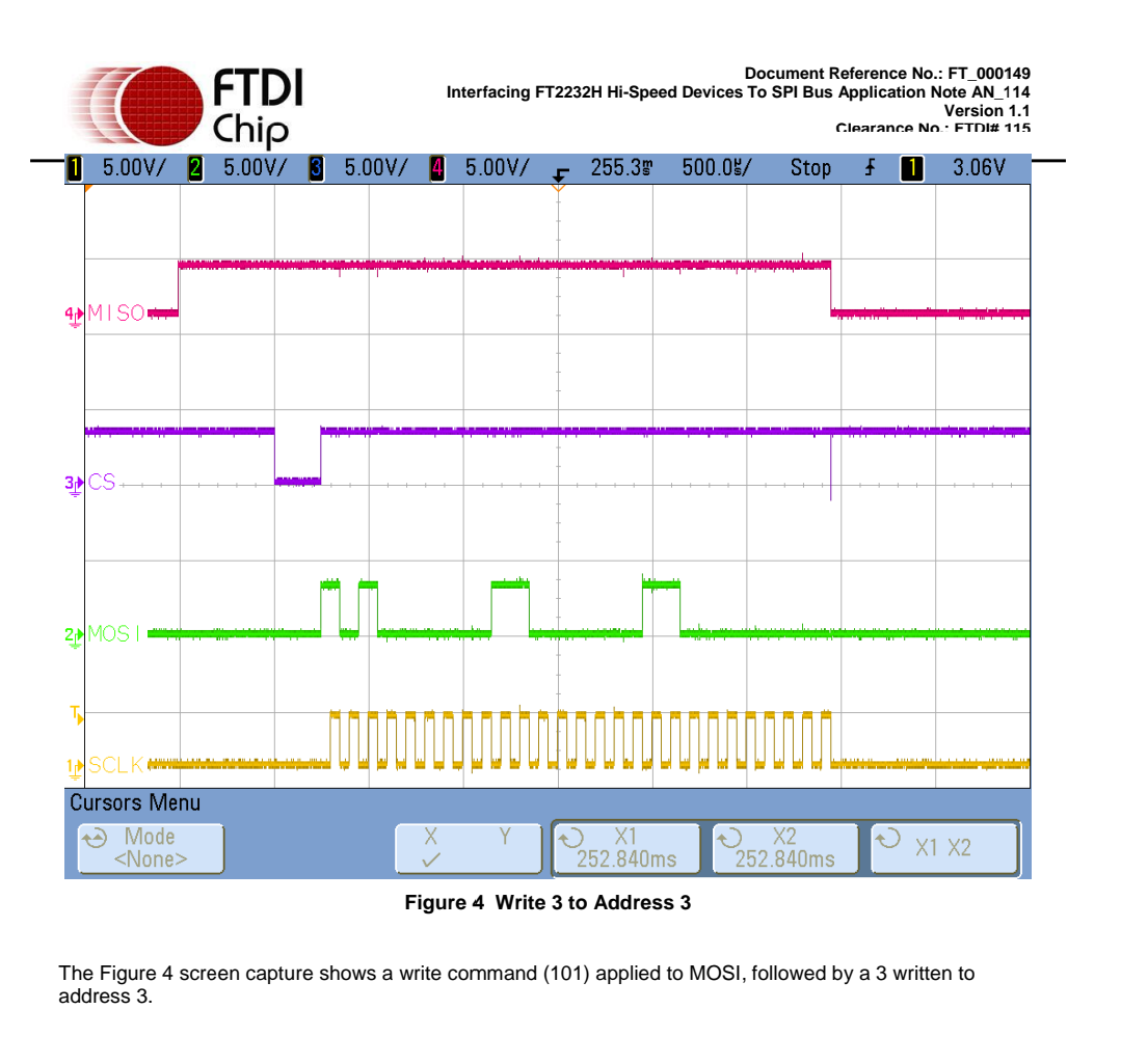
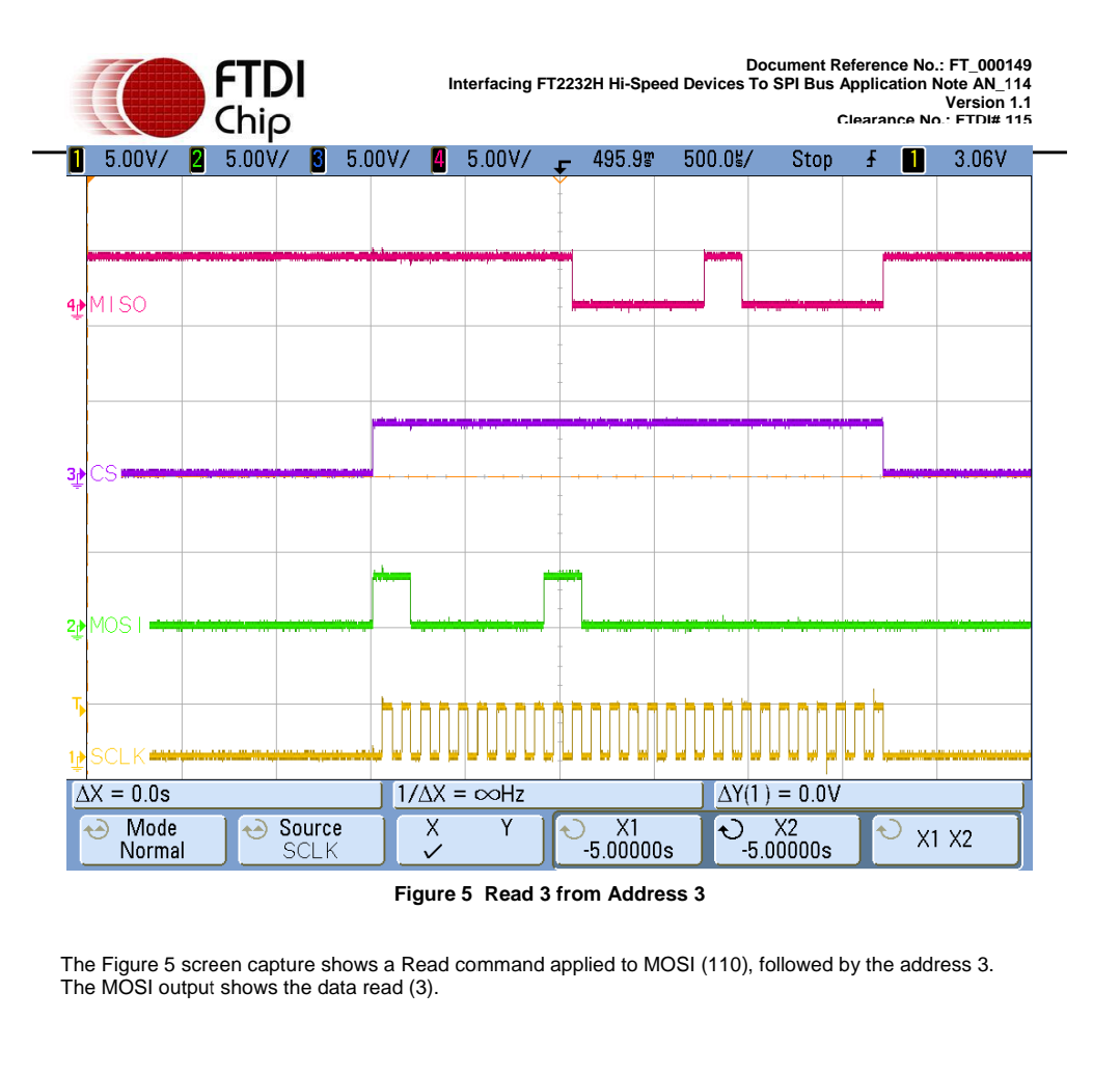
3.2 FT2232H to 93LC56 Read/Write Timing on Scope
The following screenshots show examples of the Read and write waveforms on the SPI interface. These are provided to illustrate the operational details of the SPI write and read commands sent from the FT2232H to the 93LC56 EEPROM:

 浙公网安备 33010602011771号