Electrical(Hardware) Protocols: FIFO / Pmod™ / JTAG及常用插座(20pin,14pin,10pin)插头类型及针序/ SPI / IIC / IIS / UART / SWD / ICSP / CANBus/ModBus
LVCMOS: Low Voltage COMS
LVTTL: Low Voltage TTL
Electrical(Hardware) Protocols:
0. Pmod™: innovated by DIGILENT Inc., Digilent Pmod™ Interface Specification
https://digilent.com/reference/pmod/start
https://lab.cs.tsinghua.edu.cn/digital-design/doc/hardware/peripheral/
https://www.intel.cn/content/www/cn/zh/docs/programmable/683460/current/pmod-connectors.html
The Digilent Pmod interface is used to connect low frequency, low I/O pin count peripheral modules to host
controller boards.
There are six-pin and twelve-pins versions of the interface defined,
encompassing FIFO, JTAG, SPI, I²C, UART, I²S, H-bridge and GPIO protocols. The six-pin version provides four digital I/O signal pins, one power pin and one ground pin. The twelve-pin version provides eight I/O signal pins, two power pins and two ground pins. The signals of the twelve-pin version are arranged so that it provides two of the six-pin interfaces stacked. In general, Pmod modules can plug directly into connectors on the host controller board, called host ports, or be connected to the controller board via six-pin or twelve-pin cables.
Pmod modules are powered by the host via the interface's power and ground pins.
The Pmod interface is not intended for high frequency operation, however, using RJ45 connectors and twisted pair Ethernet cable, signals have been sent reliably at 24 MHz and distances of up to 4 meters. Theoretically, signal speeds greater than 100 MHz should be achievable using high-speed ports wit
The digital signal characteristics are not specified. However, the general expectation is that a 3.3 V logic power
supply will be used and the signals will conform to LVCMOS 3.3 V or LVTTL 3.3 V logic conventions.
- JTAG(Joint Test Action Group), JTAG is actually a protocol over SPI.
5 pins/connections(GND, TMS, TCK, TDI, TDO),
Output type: Maximum voltage: 5.5volts (5volt safe), 3.3volt normal, or open collector (pull-up resistors required).
Pull-up resistors: required for open collector output mode (2K – 10K). - SPI(Serial Peripheral Interface): Innovated by MOTOROLA Inc.,
5 pins/connections(GND, CS、SCK、MISO、MOSI), - SWD(Serial Wire Debug): ARM debug interface,
3 pins/connections(GND, SWDCLK, SWDIO), - IIC(Inter-Integrated Circuits): Innovated by PHILIPS Inc.,
3 pins/connections(GND, SCL, SDA), - UART(Universal Asynchronous Receiver/Transmitter,Serial, RS232/485)
4 pins/connections(GND, RX, TX, VCC:OnlyWhenActAsPowerSource), - FIFO: High bandwidth, High transmit rate: CPU/Video/Camera FIFO
- IIS/I2S(Integrate Interface of Sound), Innovated by PHILIPS Inc. for Digital Audio devices use,
5 pins/connections(GND, DI, DO, CLK, LRCK), - ICSP: 多用于Microchip
- CAN bus / ModBus : usually Industrial/Automotive application
Serial Bus 有Sync./Async., Duplex/Half-Duplex, Bidirection/SingleDirection 三类Categories.
Serial Bus因占用较少管脚被广泛应用, 几乎所有的CPU/MCU/MicroController都有SPI/I2C和UART接口,而且不止一个。
过去几十年有3种最常用的SPI、I2C和UART; 这3种串行总线的主要区别:
- SPI - Serial Peripheral Interface(串行外设接口), 有时钟同步串行总线, Motorola 首创;
有leader/follwer之分,只有一个leader, 其他为follwer, follwer器件寻址是靠专用SS(片选信号)线实现;
信号线不需要电阻上拉; - I2C - Inter-Integrated Circuits(集成电路之间的连接), 有时钟同步串行总线, Philips 首创;
没Leader/Follwer之分, 所有挂在总线上的器件都是平等的,都有唯一的地址(身份证护照);
信号线要通过电阻上拉; - UART - Universal Asynchronous Receiver/Transmitter(通用异步收/发串行总线, 不必用时钟同步信号)。
由于很多芯片都采用管脚功能复用, 同一个管脚既用于SPI,也用于I2C,根据具体连接方式进行选用。
当器件的管脚配置为I2C时,要记住在I2C的两线(SCL、SDA)上一定要有上拉电阻,SPI则不需要。
SPI(Serial Peripheral Interface - 串行外设接口)是一种用于短距离通信(大多嵌入式系统)的同步串行通信接口规范,
这种接口由Motorola发明,已经成了一种事实标准。广泛用于各种处理器, 传感器, 串行ADC、DAC、存储器、SD卡以及LCD等进行数据连接。
JTAG: JTAG Connectors and Interfaces
November 23, 2020 by Sam Gallagher
Learn about the interfaces and connectors used to implement JTAG.
In previous articles, we’ve taken a look at the original JTAG standard, IEEE 1149.1. This included the JTAG test access port (TAP), which allows the user to manipulate a state machine to access device internals and to run boundary-scan tests.
But while this information is essential for understanding JTAG, it is also necessary to understand the physical side, including the connectors and pinouts, and the commercial JTAG interfaces available on the market. In this article, we’re going to remedy the situation, taking a less theoretical approach to JTAG as a whole.
JTAG Connectors
There is no standard connector for JTAG. More often than not, the “JTAG connector” is a standard male header, such as a 0.1” header or a finer pitch header. As we have seen, there are only four (or five) pins required to operate a JTAG TAP. However, a device which is used to ‘communicate’ with the TAP—called a JTAG interface—also needs power and ground connections, and designers can include other connections on the JTAG header if they desire.
So, given a board, how should a designer provide JTAG access? And, given a new board, where should you look to find the JTAG connector?
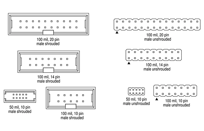
Although there is no one standard header for JTAG interfaces, several header types have become more or less standardized among manufacturers. These include the ARM JTAG 20, the ARM JTAG 14, the TI JTAG 14, the STDC14 from STMicroelectronics, the OCDS 16-pin header [pdf] from Infineon, the CoreSight 10, the CoreSight 20, the MIPI 34, and the Mictor 38. Segger defines their J-Link and J-Trace connectors to be nearly identical to the ARM JTAG 20.
Most headers are shrouded or unshrouded male headers, with 10, 14, or 20 pins, and 0.1” or 0.05” pin pitch. Examples are shown in Figure 1.
The pinouts for various JTAG interfaces (linked above) are shown in Figure 2. Here you’ll find the standard pins for JTAG (TDI, TDO, TCK, TMS, nTRST), as well as serial wire debug (SWDIO, SWCLK, SWO), and additional functions for debugging, like core tracing.
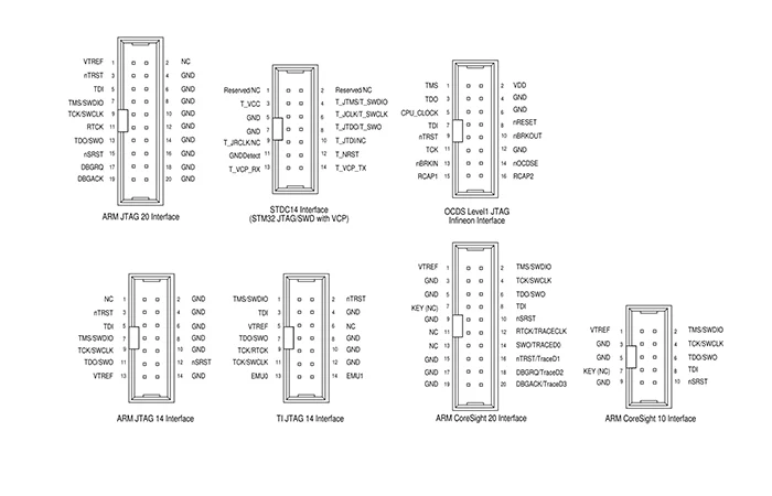
Particularly notable among the added pins are nSRST (full system reset), which forces the target to fully reset, and VTREF (voltage target reference), connected to the target supply rail for JTAG interface hardware level-shifting.
JTAG Interfaces
Several JTAG interfaces (also called JTAG debug probes) are available on the market. In the open-source hardware arena, there is the Black Magic Probe or BMP, developed by 1BitSquared and Black Sphere Technologies, used as an ARM JTAG interface, which has a large and active community supporting it. Black Magic Probe can also refer to any JTAG interface which has had its firmware replaced with the Black Magic Probe firmware.
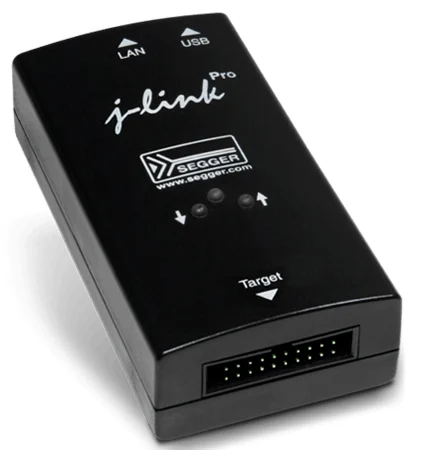
The commercial, widely used debug probes from Segger include the J-Link (shown in Figure 3) and the J-Trace, a considerably more advanced and capable debug probe suitable for industrial applications.
Specific vendors will also sell JTAG interfaces for their products. STMicroelectronics provides the STLINK series (including the STLINK/V2, and the STLINK-V3SET) for their STM8 and STM32 products, Atmel (now Microchip) provides the Atmel-ICE, NXP has the S32 Debug Probe—the list goes on.
FPGAs also use JTAG to download bit streams onto devices/memories, but these interfaces are more often called download cables. Examples include Xilinx’s Platform Cable II and Altera’s FPGA download cable, formerly known as the USB-Blaster II, now rebranded as the Intel FPGA Download Cable II.
So what exactly is going on in these devices that makes them so expensive? What functions do they support, and how does a designer use them? Generally, if you look inside a low-end debug probe, you’ll find the following:
A microcontroller as the main JTAG controller
A USB interface, which may be embedded in the microcontroller or may come separately in, for example, an FTDI chip
Level shifting circuitry for logic compatibility
Switching circuitry for enabling and disabling different paths, pull-ups, etc.
And that’s about it. As an example, look at the Black Magic Probe hardware files, available on Github. Much of the work (and cost) comes on the software end, providing powerful (sometimes real-time) debugging tools that allow a developer to make the most of the Arm CoreSight architecture.
Conclusion
To this point, we have covered the JTAG standard, including the test access port (TAP) and its state machine. In this article, we took a look at the physical side of JTAG, investigating the connectors and interfaces available to the designer from the open-source up to the commercial high-end.
From here, all that remains is a closer look at the Arm CoreSight architecture and its debug interface (ADI), which will include the increasingly common serial wire debug (SWD) JTAG alternative.
RELATED CONTENT
The JTAG Test Access Port (TAP) State Machine
JTAG Implementation in Arm Core Devices
Introduction to JTAG and the Test Access Port (TAP)
Rotary Controls For Modern Hardware Interfaces
Amphenol RF HD-EFI Series Micro-Miniature Interface Connectors | New Product Brief
What Is A JTAG Connector?

 浙公网安备 33010602011771号