
P MOS 和 N MOS
近来我找到一个我觉得是最好的关于 N-MOS P-MOS的资料, 找到了一个资料, 我感觉应该是讲的很详细了. https://www.homofaciens.de/technics-physical-computing-P-channel-MOSFETs_en.htm 我做为一个学习者, 一边翻译, 一边做记录.
 |
实物图The naming of the pins of a P-channel MOSFET is identical to that of an N-channel MOSFET. Here, too the names are Source, Drain and Gate. An IRLZ34N (N-channel) and an IRF9Z34N (P-channel) MOSFET are shown here. The assignment of the pins of both transistors is identical, but this does not always have to be the case. A look at the data sheet is essential to identify the pins! P 沟道 MOSFET 引脚的命名与 N 沟道 MOSFET 相同。这里的名称也是源极、漏极和栅极。这里显示的是 IRLZ34N(N 沟道)和 IRF9Z34N(P 沟道)MOSFET。这两个晶体管的引脚分配完全相同,但并非总是如此。要识别引脚,必须查看数据表! |
 |
At the latest when connecting a P-channel MOSFET, the differences to an N-channel MOSFET have to be kept in mind: 接线方法
|
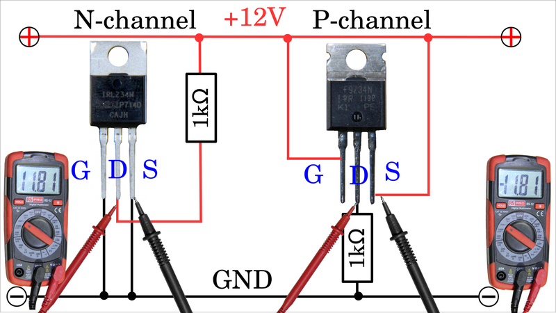 |
This becomes clear when a multimeter is used for voltage measurement. The red probe is connected to the drain pin of each MOSFET, the black probe to the source pin. It can be seen that when the transistor is switched off (0V across the gate-source path), almost the entire supply voltage of 12V drops across the drain-source path of each MOSFET, but the value at the P-channel MOSFET is displayed with a negative sign. 验证将N MOS, 和 P MOS 按照上图的方式连接, 用万用表量测结果如左图所示. |
 |
Same as with N-channel MOSFETs, the resistance of the drain-source path changes on changing gate-source voltage. Here too, the resistance for enhancement types is maximum if the potential difference between gate and source is 0V which is the case when the entire supply voltage is present between gate and ground of the P-channel MOSFET. At the N-channel MOSFET to the left there is 0V between gate and ground and between the positive supply voltage and gate pin the entire supply voltage can be measured. Both MOSFETSs are switched off, the resistance of the drain-source path is in the range of one megohm, which means that the total supply voltage drops more or less across the transistors that form a voltage divider with the 1kΩ resistors: 开关P MOS 和 N MOS一样, Rds 随着 Vgs 的电压变化而变化, 如果用N MOS 和 P MOS 都带一个 1000R 的负载. 左边的接线图. Vgs = 0v, N,P MOS管都是内阻无限大, 类似断开N-MOS, Vg = 0v, 电源 + 和 Vg 之间为 12V. N-MOS 内阻最大约1MΩ, 也可以认为 N - MOS 断开. P-MOS, Vg = 12v, Source 与电源正连接, Vg的电压为 12V. |

 浙公网安备 33010602011771号