EDP转换IC NCS8801S:RGB/LVDS转EDP芯片
RGB/LVDS-to-eDP Converter
1 Features
Embedded-DisplayPort (eDP) Output
2-lane/4-lane eDP @ 1.62/2.7Gbps per lane
FHD to WQXGA (2560*1600) supported
Up to 6dB pre-emphasis
RGB Input
18/24bit RGB Interface
Pixel clock up to 270MHz
SDR/DDR supported
Pin order reversal supported
LVDS Input
Dual-channel 6/8bit LVDS (Sync) interface
400Mbps to 1Gbps per data pair
Built-in termination
Channel and polarity swap supported
Reference Clock
Any freq. between 19MHz and 100MHz
Crystal or single-ended clock input
Built-in 5000ppm SSC generator
Misc
I2C/SPI for chip configuration
Built-in eDP handshake protocol
I2C-AUX channel for TCON/DPCD/EDID control
Built-in video test pattern
Power
1.2V core supply
2.5V or 3.3V IO supply
RGB IO can go down to 1.8V
Power consumption ~ 150mW
@ 2048*1536*24bit*60Hz, LVDS mode
Deep-sleep mode power <1mW
Package
QFN-56 (7mm x 7mm) package
RoHS Compliant
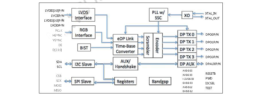
2 Block Diagram
3 General Description
NCS8801S is a low-power RGB/LVDS-to-DisplayPort/eDP converter, which is designed for mobile devices including smartphones, tablets, laptops, etc. to support high-definition DP/eDP displays.
NCS8801S supports 4-lane DP/eDP output which is typically required to support QXGA (2048*1536) and above at 60Hz frame rate.
All the functions including both RGB and LVDS interfaces pack into a small 7mm*7mm QFN56 package which saves the precious space in mobile devices.
4 Pin Diagram
NCS8801S is fully compliant with NCS8801.
...