HDLBits Verilog(3)——Karnaugh Map to Circuit
----- 73. 3-varible -----
Problem Statement
(三变量卡诺图)
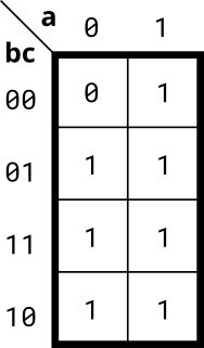
Implement the circuit described by the Karnaugh map below.
Answer
一个非常容易化简的卡诺图,因此这里仅放出化简后的逻辑表达式,图就不放了:
out' = a'b'c' or out = (a'b'c')' (撇号表示取反,乘积表示与运算,加法表示或运算)
module top_module(
    input a,
    input b,
    input c,
    output out  );

    assign out = ~(~a & ~b & ~c);

endmodule
----- 74. 4-varible (a) -----
Problem Statement
(四变量卡诺图)
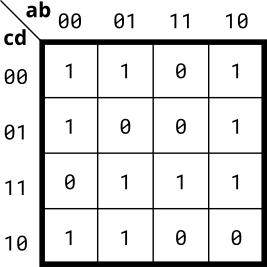
Implement the circuit described by the Karnaugh map below.
Answer
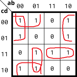
out = a'd' + b'c' + a'bc + acd
module top_module(
    input a,
    input b,
    input c,
    input d,
    output out  );

    assign out = (~a & ~d) | (~b & ~c) | (~a & b & c) | (a & c & d);

endmodule
----- 75. 4-varible (b) -----
Problem Statement
(四变量带有约束条件的卡诺图)
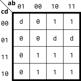
Implement the circuit described by the Karnaugh map below.
Answer
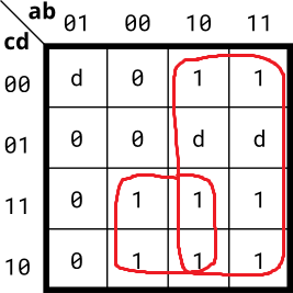
out = b'c + a
module top_module(
    input a,
    input b,
    input c,
    input d,
    output out  );

    assign out = (~b & c) | a;

endmodule
----- 76. 4-varible (c) -----
Problem Statement
(四变量卡诺图)
Implement the circuit described by the Karnaugh map below.
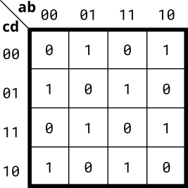
Answer
(这道题貌似只能硬解,但是也有更巧妙的办法,如下所示)
module top_module(
    input a,
    input b,
    input c,
    input d,
    output out  );

    assign out = a + b + c + d;

endmodule
----- 77. Minimum SOP and POS -----
Problem Statement
A single-output digital system with four inputs (a,b,c,d) generates a logic-1 when 2, 7, or 15 appears on the inputs, and a logic-0 when 0, 1, 4, 5, 6, 9, 10, 13, or 14 appears. The input conditions for the numbers 3, 8, 11, and 12 never occur in this system. For example, 7 corresponds to a,b,c,d being set to 0,1,1,1, respectively.
Determine the output out_sop in minimum SOP(Sum of Product,最小项表达式(与或式):积之和) form, and the output out_pos in minimum POS(Product of Sum,最大项表达式(或与式):和之积) form.
Answer
由题意画出卡诺图:
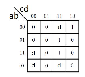
化简卡诺图:
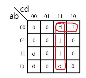
out_sop = cd + a'b'c
out_pos = ( (c'+ d')·(a + b + c') )'
(POS式我懒得化简了。。。)
module top_module (
    input a,
    input b,
    input c,
    input d,
    output out_sop,
    output out_pos
);

    assign out_sop = (c & d) | (~a & ~b & c);
	assign out_pos = ~( (~c | ~d) & (a | b | ~c) );

endmodule
----- 78. Karnaugh map (a) -----
Problem Statement
Consider the function f shown in the Karnaugh map below.
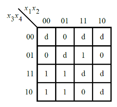
Implement this function. d is don't-care, which means you may choose to output whatever value is convenient.
Answer
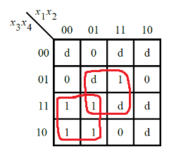
f = x1'x3 + x2x4
module top_module (
    input [4:1] x,
    output f );

    assign f = (~x[1] & x[3]) | (x[2] & x[4]);

endmodule
----- 79. Karnaugh map (b) -----
Problem Statement
Consider the function f shown in the Karnaugh map below. Implement this function.
(The original exam question asked for simplified SOP and POS forms of the function.)
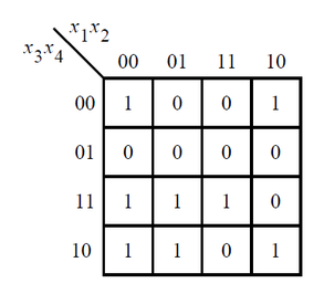
Answer

f = x2'x4' + x1'x3 + x2x3x4
module top_module (
    input [4:1] x,
    output f
);

    assign f = (~x[2] & ~x[4]) | (~x[1] & x[3]) | (x[2] & x[3] & x[4]);

endmodule
----- 80. K-map implemented with a multiplexer -----
Problem Statement
(批注:比较新颖的题目,用多路选择器实现卡诺图运算。需要注意的是,题目仅要求写出c、d的实现,并且只能使用多个二选一)
For the following Karnaugh map, give the circuit implementation(实现,执行) using one 4-to-1 multiplexer and as many 2-to-1 multiplexers as required, but using as few as possible. You are not allowed to use any other logic gate and you must use a and b as the multiplexer selector inputs, as shown on the 4-to-1 multiplexer below.
You are implementing(实现) just the portion labelled top_module, such that the entire circuit (including the 4-to-1 mux) implements the K-map.
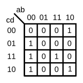

(The requirement to use only 2-to-1 multiplexers exists because the original exam question also wanted to test logic function simplification using K-maps and how to synthesize logic functions using only multiplexers with constant inputs. If you wish to treat this as purely a Verilog exercise, you may ignore this constraint and write the module any way you wish.)
Answer
(本题思路灵感来源于《FPGA原理和结构》P57,可查阅“香农展开定理”)
先说一下初步的思路:观察卡诺图,可以这么看,当cd = 00时,mux[3:0] = 0100(注意卡诺图的顺序和代码的不一致);当cd = 01时,mux[3:0] = 0001;当cd = 10时,mux[3:0] = 0101;当cd = 11时,mux[3:0] = 1001。
初步思路有了以后,其实大家已经发现了,这就是一个类似于选择器一样的东西,即输入cd,根据cd的值来输出对应mux的值。不过问题在于,我们要使用的是二选一选择器,而且应该至少要使用4个吧。列出表总结一下:
| cd | mux[3] (f3) | mux[2] (f2) | mux[1] (f1) | mux[0] (f0) |
|---|---|---|---|---|
| 00 | 0 | 1 | 0 | 0 |
| 01 | 0 | 0 | 0 | 1 |
| 10 | 0 | 1 | 0 | 1 |
| 11 | 1 | 0 | 0 | 1 |
接着我们照表写出四个逻辑表达式:
f3 = cd
f2 = c'd' + cd' = d'
f1 = 0 (这个最简单了嘿嘿)
f0 = (c'd')' = c + d
然后需要将以上四个逻辑表达式化为二选一表达式(即f = sel'·a + sel·b的形式):
f3 = c·d (对照二选一表达式:sel = c, a = 0, b = d)
f2 = d' (对照二选一表达式:sel = d, a = 1, b = 0)
f1 = 0 (不需要使用选择器了)
f0 = c + d (暂时还想不到用二选一实现的办法,直接用或门吧)
最后实现电路:
module top_module (
    input c,
    input d,
    output [3:0] mux_in
);

     mux21 ex3(.sel(c), .a(0), .b(d), .out(mux_in[3]));
	 mux21 ex2(.sel(d), .a(1), .b(0), .out(mux_in[2]));
	 assign mux_in[1] = 0;
	 assign mux_in[0] = c | d;

endmodule

module mux21 (
	input sel,
	input a, b,
	output reg out
);
	always @(*) begin
		case(sel)
			1'b0: out = a;
			1'b1: out = b;
		endcase
	end
endmodule


 浙公网安备 33010602011771号