浅析 x86 架构中 cache 的组织结构-每个程序员都应该了解的 CPU 高速缓存
cache通常被翻译为高速缓冲存储器(以下简称“高速缓存”),虽然现在cache的含义已经不单单指CPU和主存储器(也就是通常所谓的内存)之间的高速缓存了,但在本文中所谓的cache依旧特指CPU和主存储器之间的高速缓存。
这篇文章诞生的源头是我之前在stackoverflow看到的一个问题:
Why is transposing a matrix of 512×512 much slower than transposing a matrix of 513×513 ?
这个问题虽然国外的大神给出了完美的解释,但是我当时看过之后还是一头雾水。想必对x86架构上的cache没有较深入了解过的童鞋看过之后也是一样的感受吧。于是趁着寒假回家第一天还没有过多外界干扰的时候,我们就来详细的研究下x86架构下cache的组织方式吧。
我们就由这个问题开始讨论吧。这个问题说为什么转置一个512×512的矩阵反倒比513×513的矩阵要慢?(不知道什么是矩阵转置的童鞋补习线性代数去)提问者给出了测试的代码以及执行的时间。
不过我们不知道提问者测试机器的硬件架构,不过我的测试环境就是我这台笔记本了,x86架构,处理器是Intel Core i3-2310M 2.10GHz。顺便啰嗦一句,在linux下,直接用cat命令查看/proc/cpuinfo这个虚拟文件就可以查看到当前CPU的很多信息。
首先,我们将提问者给出的代码修改为C语言版,然后编译运行进行测试。提问者所给出的这段代码有逻辑问题,但是这和我们的讨论主题无关,所以请无视这些细节吧 :),代码如下:
1
|
|
我的机器上得出了如下的测试结果:
Average for a matrix of 513 : 0.003879 s
Average for a matrix of 512 : 0.004570 s
512×512的矩阵转置确实慢于513×513的矩阵,但是有意思的是我并没有提问者那么悬殊的执行结果。不过在编译命令行加上参数 -O2 优化后差异很明显了:
Average for a matrix of 513 : 0.001442 s
Average for a matrix of 512 : 0.005469 s
也就是说512×512的矩阵居然比513×513的矩阵转置平均慢了近4倍!
那么,是什么原因导致这个神奇的结果呢?
- 如果真是cache的缘故,那么cache又是如何影响代码执行的效率呢?
- 如果是因为cache具体的组织方式带来的特殊现象,那cache究竟是怎么组织的呢?
- 除此之外,仅仅是512×512的矩阵转置慢吗?其它的数字又会怎样呢?
- 搞明白了cache的组织方式之后,能给我们平时写代码定义变量有怎样的启示呢?
好了,我们提出的问题足够多了,现在我们来尝试在探索中逐一解答这些问题,并尝试分析一些现代CPU的特性对代码执行造成的影响。
我们从cache的原理说起,cache存在的目的是在高速的CPU和较低速的主存储器之间建立一个数据存储的缓冲地带,通常由SRAM制造,访问速度略慢于CPU的寄存器,但是却高于DRAM制造的主存储器。因为制造成本过高,所以cache的容量一般都很小,一般只有几MB甚至几十到几百KB而已。那你可能会说,这么小的cache怎么可能有大作用。有趣的是还真有大作用,由于程序的局部性原理的存在,小容量的cache在工作时能轻易达到90%以上的读写命中率。局部性原理分为时间局部性和空间局部性,这里不再详述,有兴趣的童鞋请参阅其他资料。
顺便插一句嘴,不光金字塔型的存储器体系结构和制造成本相关,甚至我觉得计算机体系结构很大程度受制于成本等因素的考量。假设主存储器的存储速率能和CPU寄存器比肩的话,cache肯定就会退出历史的舞台了。如果磁盘的读写速度能达到寄存器级别并且随机存取,那恐怕内存也就没有存在的必要的……
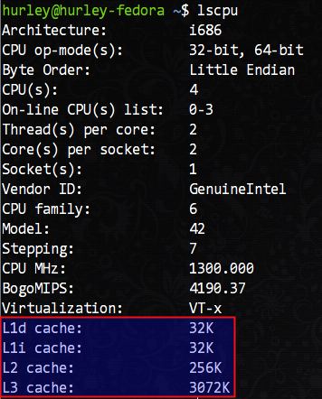
言归正传,我们如何查看自己机器上CPU的cache信息呢?/proc/cpuinfo这里是没有的,我们需要使用lscpu命令查看,这条命令在我的机器上得到了如下的输出结果:
可以看到,我的机器拥有L1d(L1数据cache)和L1i(L1指令cache)各32KB、L2 cache 256KB、L3 cache 3072KB(3MB)。
L1缓存居然分为数据缓存和指令缓存,这不是哈佛架构么?x86不是冯·诺伊曼架构么,怎么会在存储区域区分指令和数据?其实,教科书中讲述的都是完全理想化的模型,在实际的工程中,很难找到这种理想化的设计。就拿操作系统内核而言,尽管所谓的微内核组织结构更好,但是在目前所有知名的操作系统中是找不到完全符合学术意义上的微内核的例子。工程上某些时候就是一种折衷,选择更“接地气”的做法,而不是一味的契合理论模型。
既然cache容量很有限,那么如何组织数据便是重点了。接下来,我们谈谈cache和内存数据的映射方式。一般而言,有所谓的全相联映射,直接相联映射和组相联映射三种方式。
CPU和cache是以字为单位进行数据交换的,而cache却是以行(块)(即Cache Block,或Cache Line)为单位进行数据交换的。在cache中划分若干个字为一行,在内存中划分若干个字为一块,这里的行和块是大小相等的。CPU要获取某内存地址的数据时会先检查该地址所在的块是否在cache中,如果在称之为cache命中,CPU很快就可以读取到所需数据;反之称为cache未命中,此时需要从内存读取数据,同时会将该地址所在的整个内存块复制到cache里存储以备再次使用。
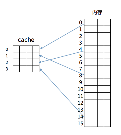
我们依次来看这三种映射方式,首先是全相联映射,这种映射方式很简单,内存中的任意一块都可以放置到cache中的任意一行去。为了便于说明,我们给出以下的简单模型来理解这个设计。
我们假设有一个4行的cache,每行4个字,每个字占4个字节,即64字节的容量。另外还有256字节(16块,每块4字,每字4字节)的一个RAM存储器来和这个cache进行映射。映射结构如图所示:
那么如何判断cache是否命中呢?由于内存和cache是多对一的映射,所以必须在cache存储一行数据的同时标示出这些数据在内存中的确切位置。简单的说,在cache每一行中都有一个Index,这个Index记录着该行数据来自内存的哪一块(其实还有若干标志位,包括有效位(valid bit)、脏位(dirty bit)、使用位(use bit)等。这些位在保证正确性、排除冲突、优化性能等方面起着重要作用)。那么在进行一个地址的判断时,采用全相联方式的话,因为任意一行都有可能存在所需数据,所以需要比较每一行的索引值才能确定cache中是否存在所需数据。这样的电路延迟较长,设计困难且复杂性高,所以一般只有在特殊场合,比如cache很小时才会使用。
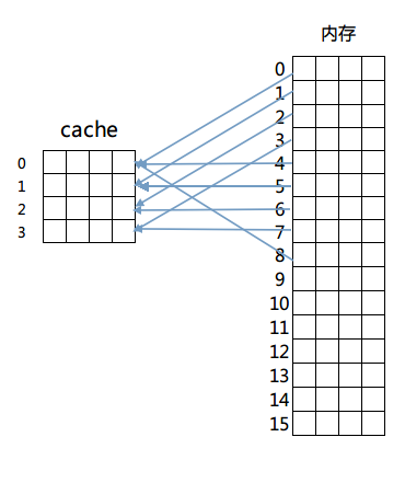
然后是第二种方法:直接相连映射。这个方法固定了行和块的对应关系,例如内存第0块必须放在cache第0行,第一块必须放在第一行,第二块必须放在第二行……循环放置,即满足公式:
内存块放置行号 = 内存块号 % cache总行数
映射如图所示:
这样做解决了比较起来困难的问题,由于每一块固定到了某一行,只需要计算出目标内存所在的行号进行检查即可判断出cache是否命中。但是这么做的话因为一旦发生冲突就必须换出cache中的指定行,频繁的更换缓存内容造成了大量延迟,而且未能有效利用程序运行期所具有的时间局部性。
综上,最终的解决方案是最后的组相联映射方式(Set Associativity),这个方案结合了以上两种映射方式的优点。具体的方法是先将cache的行进行分组,然后内存块按照组号求模来决定该内存块放置到cache的哪一个组。但是具体放置在组内哪一行都可以,具体由cache替换算法决定。
我们依旧以上面的例子来说明,将cache里的4行分为两组,然后采用内存里的块号对组号求模的方式进行组号判断,即内存0号块第一组里,2号块放置在第二组里,3号块又放置在第一组,以此类推。这么做的话,在组内发生冲突的话,可以选择换出组内一个不经常读写的内存块,从而减少冲突,更好的利用了资源(具体的cache替换策略不在讨论范围内,有兴趣的童鞋请自行研究)。同时因为组内行数不会很多,也避免了电路延迟和设计的复杂性。
x86中cache的组织方式采用的便是组相联映射方式。
上面的阐述可能过于简单,不过大家应该理解了组相联映射方式是怎么回事了。那么我们接下来结合我的机器上具体的cache映射计算方法继续分析。
我们刚说过组相联映射方式的行号可以通过 块号 % 分组个数 的公式来计算,那么直接给出一个内存地址的话如何计算呢?其实内存地址所在的块号就是 内存地址值 / 分块字节数,那么直接由一个内存地址计算出所在cache中的行分组的组号计算公式就是:
内存地址所在cache组号 = (内存地址值 / 分块字节数) % 分组个数
很简单吧?假定一个cache行(内存块)有4个字,我们画出一个32位地址拆分后的样子:
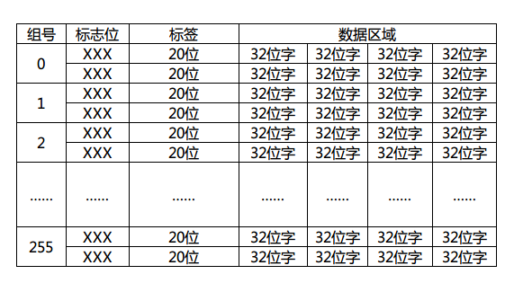
因为字长32的话,每个字有4个字节,所以需要内存地址最低2位时字节偏移,同理每行(块)有4个字,块内偏移也是2位。这里的索引位数取决于cache里的行数,这个图里我画了8位,那就表示cache一共有256个分组(0~255)存在,每个分组有多少行呢?这个随意了,这里的行数是N,cache就是N路组相联映射。具体的判断自然是取tag进行组内逐一匹配测试了,如果不幸没有命中,那就需要按照cache替换算法换出组内的一行了。顺带画出这个地址对应的cache结构图:
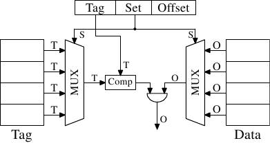
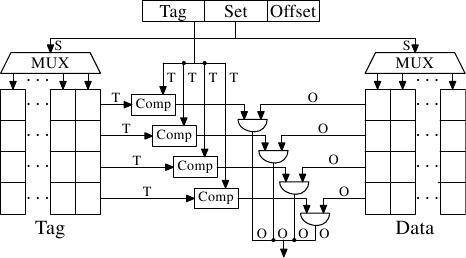
标志位是有效位(valid bit)、脏位(dirty bit)、使用位(use bit)等,用于该cache行的写回算法,替换算法使用。这里简单期间我就画了一个2路组相联映射的例子出来。现在大家应该大致明白cache工作的流程了吧?首先由给出的内存地址计算出所在cache的组号(索引),再由判断电路逐一比较标签(tag)值来判断是否命中,若命中则通过行(块)内偏移返回所在字数据,否则由cache替换算法决定换出某一行(块),同时由内存调出该行(块)数据进行替换。
其实工作的流程就是这样,至于cache写回的策略(写回法,写一次法,全写法)不在本文的讨论范围之内,就不细说了。
有了以上铺垫,我们终于可以来解释那个512×512的矩阵转置问题了。很艰难的铺垫,不是吗?但我们距离胜利越来越近了。
512×512的矩阵,或者用C语言的说法称之为512×512的整型二维数组,在内存中是按顺序存储的。
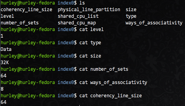
那么以我的机器为例,在上面的lscpu命令输出的结果中,L1d(一级数据缓存)拥有32KB的容量。但是,有没有更详细的行大小和分组数量的信息?当然有,而且不需要多余的命令。在/sys/devices/system/cpu目录下就可以看到各个CPU核的所有详细信息,当然也包括cache的详细信息,我们主要关注L1d缓存的信息,以核0为例,在/sys/devices/system/cpu/cpu0/cache目录下有index0~index4这四个目录,分别对应L1d,L1i,L2,L3的信息。我们以L1d(index0)为例查看详细参数。
从图中我们可以知道,这是L1数据缓存的相关信息:共有64个组,每组8行,每行16字(64字节),共有32KB的总容量。按照我们之前的分析,相信你很容易就能说出这个机器上L1d缓存的组织方式。没错,就是8路组相联映射。
顺带贴出Intel的官方文档证明我不是在信口开河:
此时32位内存地址的拆分如下:
对应的cache图想必也难不倒大家吧?和上边的cache结构不同的就是改变了分组数量、每组行数和每行大小。
我们继续分析转置问题。每个cache行(块)拥有64个字节,正好是16个int变量的大小。一个n阶矩阵的一个行正好填充n / 16个cache行。512阶矩阵的话,每个矩阵的行就填充了32个组中的行,2个矩阵的行就覆盖了64个组。之后的行若要使用,就必然牵扯到cache的替换了。如果此时二维数组的array[0][0]开始从cache第一行开始放置。那么当进入第二重for循环之后,由于内存地址计算出的cache组号相同,导致每一个组中的正在使用的cache行发生了替换,不断发生的组内替换使得cache完全没有发挥出效果,所以造成了512×512的矩阵在转置的时候耗时较大的原因。具体的替换点大家可以自行去计算,另外513×513矩阵大家也可以试着去分析没有过多cache失效的原因。不过这个问题是和CPU架构有关的,所以假如你的机器没有产生同样的效果,不妨自己研究研究自己机器的cache结构。
另外网上针对这个问题也有诸多大牛给出的解释,大家不妨参照着理解吧。别人说过的我就不说了,大家可以参考着分析。
原本想把这篇作为上篇,再去写一个下篇讲述一些编程中要注意的问题。不过偶然间看到了微软大牛Igor Ostrovsky的博文《Gallery of Processor Cache Effects》,瞬间感觉自己不可能写的更好了。所以推荐大家去读这篇文章。如果感觉英文吃力的话,耗子叔这里有@我的上铺叫路遥做的翻译解释《7个示例科普CPU Cache》。
另外,开源中国这里的一篇译文也有参考价值:《每个程序员都应该了解的 CPU 高速缓存》。
One quick request: in a document of this length there are bound to be a few typographical errors remaining. If you find one, and wish to see it corrected, please let us know via mail to lwn@lwn.net rather than by posting a comment. That way we will be sure to incorporate the fix and get it back into Ulrich's copy of the document and other readers will not have to plow through uninteresting comments.]
[编者按:这是Ulrich Drepper写“程序员都该知道存储器”的第二部。那些没有读过第一部 的读者可能希望从这一部开始。这本书写的非常好,并且感谢Ulrich授权我们出版。
一点说明:书籍出版时可能会有一些印刷错误,如果你发现,并且想让它在后续的出版中更正,请将意见发邮件到lwn@lwn.net ,我们一定会更正,并反馈给Ulrich的文档副本,别的读者就不会受到这些困扰。]
CPUs are today much more sophisticated than they were only 25 years ago. In those days, the frequency of the CPU core was at a level equivalent to that of the memory bus. Memory access was only a bit slower than register access. But this changed dramatically in the early 90s, when CPU designers increased the frequency of the CPU core but the frequency of the memory bus and the performance of RAM chips did not increase proportionally. This is not due to the fact that faster RAM could not be built, as explained in the previous section. It is possible but it is not economical. RAM as fast as current CPU cores is orders of magnitude more expensive than any dynamic RAM.
If the choice is between a machine with very little, very fast RAM and a machine with a lot of relatively fast RAM, the second will always win given a working set size which exceeds the small RAM size and the cost of accessing secondary storage media such as hard drives. The problem here is the speed of secondary storage, usually hard disks, which must be used to hold the swapped out part of the working set. Accessing those disks is orders of magnitude slower than even DRAM access.
Fortunately it does not have to be an all-or-nothing decision. A computer can have a small amount of high-speed SRAM in addition to the large amount of DRAM. One possible implementation would be to dedicate a certain area of the address space of the processor as containing the SRAM and the rest the DRAM. The task of the operating system would then be to optimally distribute data to make use of the SRAM. Basically, the SRAM serves in this situation as an extension of the register set of the processor.
如果有两个选项让你选择,一个是速度非常快、但容量很小的内存,一个是速度还算快、但容量很多的内存,如果你的工作集比较大,超过了前一种情况,那么人们总是会选择第二个选项。原因在于辅存(一般为磁盘)的速度。由于工作集超过主存,那么必须用辅存来保存交换出去的那部分数据,而辅存的速度往往要比主存慢上好几个数量级。
好在这问题也并不全然是非甲即乙的选择。在配置大量DRAM的同时,我们还可以配置少量SRAM。将地址空间的某个部分划给SRAM,剩下的部分划给DRAM。一般来说,SRAM可以当作扩展的寄存器来使用。
While this is a possible implementation, it is not viable. Ignoring the problem of mapping the physical resources of such SRAM-backed memory to the virtual address spaces of the processes (which by itself is terribly hard) this approach would require each process to administer in software the allocation of this memory region. The size of the memory region can vary from processor to processor (i.e., processors have different amounts of the expensive SRAM-backed memory). Each module which makes up part of a program will claim its share of the fast memory, which introduces additional costs through synchronization requirements. In short, the gains of having fast memory would be eaten up completely by the overhead of administering the resources.
So, instead of putting the SRAM under the control of the OS or user, it becomes a resource which is transparently used and administered by the processors. In this mode, SRAM is used to make temporary copies of (to cache, in other words) data in main memory which is likely to be used soon by the processor. This is possible because program code and data has temporal and spatial locality. This means that, over short periods of time, there is a good chance that the same code or data gets reused. For code this means that there are most likely loops in the code so that the same code gets executed over and over again (the perfect case for spatial locality). Data accesses are also ideally limited to small regions. Even if the memory used over short time periods is not close together there is a high chance that the same data will be reused before long (temporal locality). For code this means, for instance, that in a loop a function call is made and that function is located elsewhere in the address space. The function may be distant in memory, but calls to that function will be close in time. For data it means that the total amount of memory used at one time (the working set size) is ideally limited but the memory used, as a result of the random access nature of RAM, is not close together. Realizing that locality exists is key to the concept of CPU caches as we use them today.
A simple computation can show how effective caches can theoretically be. Assume access to main memory takes 200 cycles and access to the cache memory take 15 cycles. Then code using 100 data elements 100 times each will spend 2,000,000 cycles on memory operations if there is no cache and only 168,500 cycles if all data can be cached. That is an improvement of 91.5%.
The size of the SRAM used for caches is many times smaller than the main memory. In the author's experience with workstations with CPU caches the cache size has always been around 1/1000th of the size of the main memory (today: 4MB cache and 4GB main memory). This alone does not constitute a problem. If the size of the working set (the set of data currently worked on) is smaller than the cache size it does not matter. But computers do not have large main memories for no reason. The working set is bound to be larger than the cache. This is especially true for systems running multiple processes where the size of the working set is the sum of the sizes of all the individual processes and the kernel.
我们先用一个简单的计算来展示一下高速缓存的效率。假设,访问主存需要200个周期,而访问高速缓存需要15个周期。如果使用100个数据元素100次,那么在没有高速缓存的情况下,需要2000000个周期,而在有高速缓存、而且所有数据都已被缓存的情况下,只需要168500个周期。节约了91.5%的时间。
用作高速缓存的SRAM容量比主存小得多。以我的经验来说,高速缓存的大小一般是主存的千分之一左右(目前一般是4GB主存、4MB缓存)。这一点本身并不是什么问题。只是,计算机一般都会有比较大的主存,因此工作集的大小总是会大于缓存。特别是那些运行多进程的系统,它的工作集大小是所有进程加上内核的总和。
What is needed to deal with the limited size of the cache is a set of good strategies to determine what should be cached at any given time. Since not all data of the working set is used at exactly the same time we can use techniques to temporarily replace some data in the cache with other data. And maybe this can be done before the data is actually needed. This prefetching would remove some of the costs of accessing main memory since it happens asynchronously with respect to the execution of the program. All these techniques and more can be used to make the cache appear bigger than it actually is. We will discuss them in Section 3.3. Once all these techniques are exploited it is up to the programmer to help the processor. How this can be done will be discussed in Section 6.
3.1 CPU Caches in the Big Picture
Before diving into technical details of the implementation of CPU caches some readers might find it useful to first see in some more details how caches fit into the “big picture” of a modern computer system.
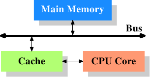
Figure 3.1: Minimum Cache Configuration
Figure 3.1 shows the minimum cache configuration. It corresponds to the architecture which could be found in early systems which deployed CPU caches. The CPU core is no longer directly connected to the main memory. {In even earlier systems the cache was attached to the system bus just like the CPU and the main memory. This was more a hack than a real solution.} All loads and stores have to go through the cache. The connection between the CPU core and the cache is a special, fast connection. In a simplified representation, the main memory and the cache are connected to the system bus which can also be used for communication with other components of the system. We introduced the system bus as “FSB” which is the name in use today; see Section 2.2. In this section we ignore the Northbridge; it is assumed to be present to facilitate the communication of the CPU(s) with the main memory.
3.1 高速缓存的位置
在深入介绍高速缓存的技术细节之前,有必要说明一下它在现代计算机系统中所处的位置。
图3.1: 最简单的高速缓存配置图
图3.1展示了最简单的高速缓存配置。早期的一些系统就是类似的架构。在这种架构中,CPU核心不再直连到主存。{在一些更早的系统中,高速缓存像CPU与主存一样连到系统总线上。那种做法更像是一种hack,而不是真正的解决方案。}数据的读取和存储都经过高速缓存。CPU核心与高速缓存之间是一条特殊的快速通道。在简化的表示法中,主存与高速缓存都连到系统总线上,这条总线同时还用于与其它组件通信。我们管这条总线叫“FSB”——就是现在称呼它的术语,参见第2.2节。在这一节里,我们将忽略北桥。
Even though computers for the last several decades have used the von Neumann architecture, experience has shown that it is of advantage to separate the caches used for code and for data. Intel has used separate code and data caches since 1993 and never looked back. The memory regions needed for code and data are pretty much independent of each other, which is why independent caches work better. In recent years another advantage emerged: the instruction decoding step for the most common processors is slow; caching decoded instructions can speed up the execution, especially when the pipeline is empty due to incorrectly predicted or impossible-to-predict branches.
Soon after the introduction of the cache, the system got more complicated. The speed difference between the cache and the main memory increased again, to a point that another level of cache was added, bigger and slower than the first-level cache. Only increasing the size of the first-level cache was not an option for economical reasons. Today, there are even machines with three levels of cache in regular use. A system with such a processor looks like Figure 3.2. With the increase on the number of cores in a single CPU the number of cache levels might increase in the future even more.
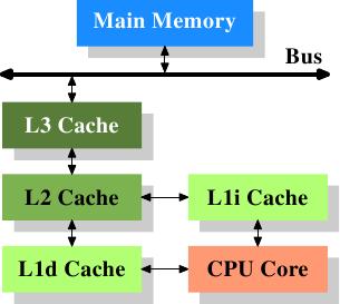
Figure 3.2: Processor with Level 3 Cache
Figure 3.2 shows three levels of cache and introduces the nomenclature we will use in the remainder of the document. L1d is the level 1 data cache, L1i the level 1 instruction cache, etc. Note that this is a schematic; the data flow in reality need not pass through any of the higher-level caches on the way from the core to the main memory. CPU designers have a lot of freedom designing the interfaces of the caches. For programmers these design choices are invisible.
在高速缓存出现后不久,系统变得更加复杂。高速缓存与主存之间的速度差异进一步拉大,直到加入了另一级缓存。新加入的这一级缓存比第一级缓存更大,但是更慢。由于加大一级缓存的做法从经济上考虑是行不通的,所以有了二级缓存,甚至现在的有些系统拥有三级缓存,如图3.2所示。随着单个CPU中核数的增加,未来甚至可能会出现更多层级的缓存。
图3.2: 三级缓存的处理器
图3.2展示了三级缓存,并介绍了本文将使用的一些术语。L1d是一级数据缓存,L1i是一级指令缓存,等等。请注意,这只是示意图,真正的数据流并不需要流经上级缓存。CPU的设计者们在设计高速缓存的接口时拥有很大的自由。而程序员是看不到这些设计选项的。
In addition we have processors which have multiple cores and each core can have multiple “threads”. The difference between a core and a thread is that separate cores have separate copies of (almost {Early multi-core processors even had separate 2nd level caches and no 3rd level cache.}) all the hardware resources. The cores can run completely independently unless they are using the same resources—e.g., the connections to the outside—at the same time. Threads, on the other hand, share almost all of the processor's resources. Intel's implementation of threads has only separate registers for the threads and even that is limited, some registers are shared. The complete picture for a modern CPU therefore looks like Figure 3.3.
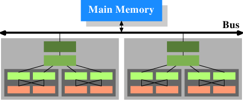
Figure 3.3: Multi processor, multi-core, multi-thread
In this figure we have two processors, each with two cores, each of which has two threads. The threads share the Level 1 caches. The cores (shaded in the darker gray) have individual Level 1 caches. All cores of the CPU share the higher-level caches. The two processors (the two big boxes shaded in the lighter gray) of course do not share any caches. All this will be important, especially when we are discussing the cache effects on multi-process and multi-thread applications.
另外,我们有多核CPU,每个核心可以有多个“线程”。核心与线程的不同之处在于,核心拥有独立的硬件资源({早期的多核CPU甚至有独立的二级缓存。})。在不同时使用相同资源(比如,通往外界的连接)的情况下,核心可以完全独立地运行。而线程只是共享资源。Intel的线程只有独立的寄存器,而且还有限制——不是所有寄存器都独立,有些是共享的。综上,现代CPU的结构就像图3.3所示。
图3.3 多处理器、多核心、多线程
在上图中,有两个处理器,每个处理器有两个核心,每个核心有两个线程。线程们共享一级缓存。核心(以深灰色表示)有独立的一级缓存,同时共享二级缓存。处理器(淡灰色)之间不共享任何缓存。这些信息很重要,特别是在讨论多进程和多线程情况下缓存的影响时尤为重要。
3.2 Cache Operation at High Level
To understand the costs and savings of using a cache we have to combine the knowledge about the machine architecture and RAM technology from Section 2 with the structure of caches described in the previous section.
By default all data read or written by the CPU cores is stored in the cache. There are memory regions which cannot be cached but this is something only the OS implementers have to be concerned about; it is not visible to the application programmer. There are also instructions which allow the programmer to deliberately bypass certain caches. This will be discussed in Section 6.
3.2 高级的缓存操作
了解成本和节约使用缓存,我们必须结合在第二节中讲到的关于计算机体系结构和RAM技术,以及前一节讲到的缓存描述来探讨。
默认情况下,CPU核心所有的数据的读或写都存储在缓存中。当然,也有内存区域不能被缓存的,但是这种情况只发生在操作系统的实现者对数据考虑的前提下;对程序实现者来说,这是不可见的。这也说明,程序设计者可以故意绕过某些缓存,不过这将是第六节中讨论的内容了。
If the CPU needs a data word the caches are searched first. Obviously, the cache cannot contain the content of the entire main memory (otherwise we would need no cache), but since all memory addresses are cacheable, each cache entry is tagged using the address of the data word in the main memory. This way a request to read or write to an address can search the caches for a matching tag. The address in this context can be either the virtual or physical address, varying based on the cache implementation.
Since the tag requires space in addition to the actual memory, it is inefficient to chose a word as the granularity of the cache. For a 32-bit word on an x86 machine the tag itself might need 32 bits or more. Furthermore, since spatial locality is one of the principles on which caches are based, it would be bad to not take this into account. Since neighboring memory is likely to be used together it should also be loaded into the cache together. Remember also what we learned in Section 2.2.1: RAM modules are much more effective if they can transport many data words in a row without a new CAS or even RAS signal. So the entries stored in the caches are not single words but, instead, “lines” of several contiguous words. In early caches these lines were 32 bytes long; now the norm is 64 bytes. If the memory bus is 64 bits wide this means 8 transfers per cache line. DDR supports this transport mode efficiently.
如果CPU需要访问某个字(word),先检索缓存。很显然,缓存不可能容纳主存所有内容(否则还需要主存干嘛)。系统用字的内存地址来对缓存条目进行标记。如果需要读写某个地址的字,那么根据标签来检索缓存即可。这里用到的地址可以是虚拟地址,也可以是物理地址,取决于缓存的具体实现。
标签是需要额外空间的,用字作为缓存的粒度显然毫无效率。比如,在x86机器上,32位字的标签可能需要32位,甚至更长。另一方面,由于空间局部性的存在,与当前地址相邻的地址有很大可能会被一起访问。再回忆下2.2.1节——内存模块在传输位于同一行上的多份数据时,由于不需要发送新CAS信号,甚至不需要发送RAS信号,因此可以实现很高的效率。基于以上的原因,缓存条目并不存储单个字,而是存储若干连续字组成的“线”。在早期的缓存中,线长是32字节,现在一般是64字节。对于64位宽的内存总线,每条线需要8次传输。而DDR对于这种传输模式的支持更为高效。
When memory content is needed by the processor the entire cache line is loaded into the L1d. The memory address for each cache line is computed by masking the address value according to the cache line size. For a 64 byte cache line this means the low 6 bits are zeroed. The discarded bits are used as the offset into the cache line. The remaining bits are in some cases used to locate the line in the cache and as the tag. In practice an address value is split into three parts. For a 32-bit address it might look as follows:
With a cache line size of 2O the low O bits are used as the offset into the cache line. The next S bits select the “cache set”. We will go into more detail soon on why sets, and not single slots, are used for cache lines. For now it is sufficient to understand there are 2S sets of cache lines. This leaves the top 32 - S - O = T bits which form the tag. These T bits are the value associated with each cache line to distinguish all the aliases {All cache lines with the same S part of the address are known by the same alias.} which are cached in the same cache set. The S bits used to address the cache set do not have to be stored since they are the same for all cache lines in the same set.
当处理器需要内存中的某块数据时,整条缓存线被装入L1d。缓存线的地址通过对内存地址进行掩码操作生成。对于64字节的缓存线,是将低6位置0。这些被丢弃的位作为线内偏移量。其它的位作为标签,并用于在缓存内定位。在实践中,我们将地址分为三个部分。32位地址的情况如下:
如果缓存线长度为2O,那么地址的低O位用作线内偏移量。上面的S位选择“缓存集”。后面我们会说明使用缓存集的原因。现在只需要明白一共有2S个缓存集就够了。剩下的32 - S - O = T位组成标签。它们用来区分别名相同的各条线{有相同S部分的缓存线被称为有相同的别名。}用于定位缓存集的S部分不需要存储,因为属于同一缓存集的所有线的S部分都是相同的。
When an instruction modifies memory the processor still has to load a cache line first because no instruction modifies an entire cache line at once (exception to the rule: write-combining as explained in Section 6.1). The content of the cache line before the write operation therefore has to be loaded. It is not possible for a cache to hold partial cache lines. A cache line which has been written to and which has not been written back to main memory is said to be “dirty”. Once it is written the dirty flag is cleared.
To be able to load new data in a cache it is almost always first necessary to make room in the cache. An eviction from L1d pushes the cache line down into L2 (which uses the same cache line size). This of course means room has to be made in L2. This in turn might push the content into L3 and ultimately into main memory. Each eviction is progressively more expensive. What is described here is the model for an exclusive cache as is preferred by modern AMD and VIA processors. Intel implements inclusive caches {This generalization is not completely correct. A few caches are exclusive and some inclusive caches have exclusive cache properties.} where each cache line in L1d is also present in L2. Therefore evicting from L1d is much faster. With enough L2 cache the disadvantage of wasting memory for content held in two places is minimal and it pays off when evicting. A possible advantage of an exclusive cache is that loading a new cache line only has to touch the L1d and not the L2, which could be faster.
当某条指令修改内存时,仍然要先装入缓存线,因为任何指令都不可能同时修改整条线(只有一个例外——第6.1节中将会介绍的写合并(write-combine))。因此需要在写操作前先把缓存线装载进来。如果缓存线被写入,但还没有写回主存,那就是所谓的“脏了”。脏了的线一旦写回主存,脏标记即被清除。
为了装入新数据,基本上总是要先在缓存中清理出位置。L1d将内容逐出L1d,推入L2(线长相同)。当然,L2也需要清理位置。于是L2将内容推入L3,最后L3将它推入主存。这种逐出操作一级比一级昂贵。这里所说的是现代AMD和VIA处理器所采用的独占型缓存(exclusive cache)。而Intel采用的是包容型缓存(inclusive cache),{并不完全正确,Intel有些缓存是独占型的,还有一些缓存具有独占型缓存的特点。}L1d的每条线同时存在于L2里。对这种缓存,逐出操作就很快了。如果有足够L2,对于相同内容存在不同地方造成内存浪费的缺点可以降到最低,而且在逐出时非常有利。而独占型缓存在装载新数据时只需要操作L1d,不需要碰L2,因此会比较快。
The CPUs are allowed to manage the caches as they like as long as the memory model defined for the processor architecture is not changed. It is, for instance, perfectly fine for a processor to take advantage of little or no memory bus activity and proactively write dirty cache lines back to main memory. The wide variety of cache architectures among the processors for the x86 and x86-64, between manufacturers and even within the models of the same manufacturer, are testament to the power of the memory model abstraction.
In symmetric multi-processor (SMP) systems the caches of the CPUs cannot work independently from each other. All processors are supposed to see the same memory content at all times. The maintenance of this uniform view of memory is called “cache coherency”. If a processor were to look simply at its own caches and main memory it would not see the content of dirty cache lines in other processors. Providing direct access to the caches of one processor from another processor would be terribly expensive and a huge bottleneck. Instead, processors detect when another processor wants to read or write to a certain cache line.
处理器体系结构中定义的作为存储器的模型只要还没有改变,那就允许多CPU按照自己的方式来管理高速缓存。这表示,例如,设计优良的处理器,利用很少或根本没有内存总线活动,并主动写回主内存脏高速缓存行。这种高速缓存架构在如x86和x86-64各种各样的处理器间存在。制造商之间,即使在同一制造商生产的产品中,证明了的内存模型抽象的力量。
在对称多处理器(SMP)架构的系统中,CPU的高速缓存不能独立的工作。在任何时候,所有的处理器都应该拥有相同的内存内容。保证这样的统一的内存视图被称为“高速缓存一致性”。如果在其自己的高速缓存和主内存间,处理器设计简单,它将不会看到在其他处理器上的脏高速缓存行的内容。从一个处理器直接访问另一个处理器的高速缓存这种模型设计代价将是非常昂贵的,它是一个相当大的瓶颈。相反,当另一个处理器要读取或写入到高速缓存线上时,处理器会去检测。
If a write access is detected and the processor has a clean copy of the cache line in its cache, this cache line is marked invalid. Future references will require the cache line to be reloaded. Note that a read access on another CPU does not necessitate an invalidation, multiple clean copies can very well be kept around.
More sophisticated cache implementations allow another possibility to happen. If the cache line which another processor wants to read from or write to is currently marked dirty in the first processor's cache a different course of action is needed. In this case the main memory is out-of-date and the requesting processor must, instead, get the cache line content from the first processor. Through snooping, the first processor notices this situation and automatically sends the requesting processor the data. This action bypasses main memory, though in some implementations the memory controller is supposed to notice this direct transfer and store the updated cache line content in main memory. If the access is for writing the first processor then invalidates its copy of the local cache line.
如果CPU检测到一个写访问,而且该CPU的cache中已经缓存了一个cache line的原始副本,那么这个cache line将被标记为无效的cache line。接下来在引用这个cache line之前,需要重新加载该cache line。需要注意的是读访问并不会导致cache line被标记为无效的。
更精确的cache实现需要考虑到其他更多的可能性,比如第二个CPU在读或者写他的cache line时,发现该cache line在第一个CPU的cache中被标记为脏数据了,此时我们就需要做进一步的处理。在这种情况下,主存储器已经失效,第二个CPU需要读取第一个CPU的cache line。通过测试,我们知道在这种情况下第一个CPU会将自己的cache line数据自动发送给第二个CPU。这种操作是绕过主存储器的,但是有时候存储控制器是可以直接将第一个CPU中的cache line数据存储到主存储器中。对第一个CPU的cache的写访问会导致本地cache line的所有拷贝被标记为无效。
Over time a number of cache coherency protocols have been developed. The most important is MESI, which we will introduce in Section 3.3.4. The outcome of all this can be summarized in a few simple rules:
- A dirty cache line is not present in any other processor's cache.
- Clean copies of the same cache line can reside in arbitrarily many caches.
If these rules can be maintained, processors can use their caches efficiently even in multi-processor systems. All the processors need to do is to monitor each others' write accesses and compare the addresses with those in their local caches. In the next section we will go into a few more details about the implementation and especially the costs.
- 一个脏缓存线不存在于任何其他处理器的缓存之中。
- 同一缓存线中的干净拷贝可以驻留在任意多个其他缓存之中。
Finally, we should at least give an impression of the costs associated with cache hits and misses. These are the numbers Intel lists for a Pentium M:
To Where Cycles Register <= 1 L1d ~3 L2 ~14 Main Memory ~240
These are the actual access times measured in CPU cycles. It is interesting to note that for the on-die L2 cache a large part (probably even the majority) of the access time is caused by wire delays. This is a physical limitation which can only get worse with increasing cache sizes. Only process shrinking (for instance, going from 60nm for Merom to 45nm for Penryn in Intel's lineup) can improve those numbers.
最后,我们至少应该关注高速缓存命中或未命中带来的消耗。下面是英特尔奔腾 M 的数据:
| To Where | Cycles |
|---|---|
| Register | <= 1 |
| L1d | ~3 |
| L2 | ~14 |
| Main Memory | ~240 |
这是在CPU周期中的实际访问时间。有趣的是,对于L2高速缓存的访问时间很大一部分(甚至是大部分)是由线路的延迟引起的。这是一个限制,增加高速缓存的大小变得更糟。只有当减小时(例如,从60纳米的Merom到45纳米Penryn处理器),可以提高这些数据。
The numbers in the table look high but, fortunately, the entire cost does not have to be paid for each occurrence of the cache load and miss. Some parts of the cost can be hidden. Today's processors all use internal pipelines of different lengths where the instructions are decoded and prepared for execution. Part of the preparation is loading values from memory (or cache) if they are transferred to a register. If the memory load operation can be started early enough in the pipeline, it may happen in parallel with other operations and the entire cost of the load might be hidden. This is often possible for L1d; for some processors with long pipelines for L2 as well.
There are many obstacles to starting the memory read early. It might be as simple as not having sufficient resources for the memory access or it might be that the final address of the load becomes available late as the result of another instruction. In these cases the load costs cannot be hidden (completely).
提早启动内存的读取有许多障碍。它可能只是简单的不具有足够资源供内存访问,或者地址从另一个指令获取,然后加载的最终地址才变得可用。在这种情况下,加载成本是不能隐藏的(完全的)。









 浙公网安备 33010602011771号