Using a Virtex Device to Drive 5V CMOS-Level Signals
Must tri-state outputs and use an external resistor to pull up to 5V
To drive 5V CMOS-level inputs, a pull-up resistor must be applied to the 5V Virtex output. Prior
to driving a logic 1 data signal, the Virtex output must be tri-stated. This ensures no overlap or
crowbar current in the input buffers of the 5V-receiving device.
The required Virtex output pin configuration is commonly called “open collector”, or more
correctly, “open drain”. This function is easily generated inside the chip by driving the data
together with the active low Output Enable signal of the output block. The external low-to-high
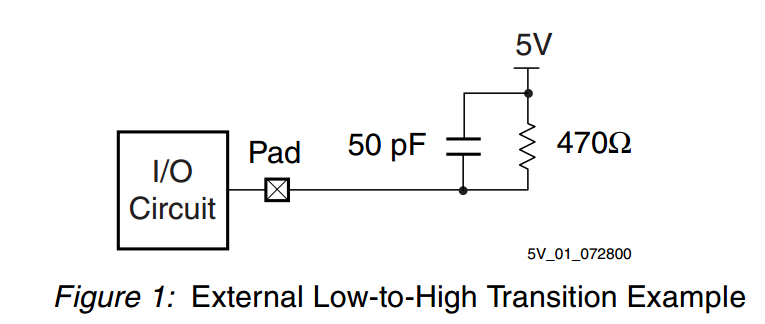
transition is then driven only by the pull-up resistor. For example, applying a 470-ohm pull-up
resistor to 5V and a 50-pF load capacitance (as shown in Figure 1) creates a 0.4V to 4.5V rise
time of about 40 ns.

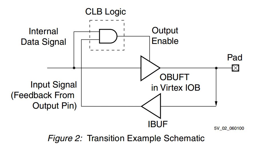
For a faster rise time, the internal active low Output Enable signal is not driven directly from the
internal data signal. Instead, it is driven from a two-input AND gate that is driven by both the
internal data signal and the input signal returned from the same device’s output pin. On the
rising edge, this assures that the output pull-up transistor is active for most of the rise time,
resulting in a shorter output delay. The important part of the rise time from 0.4V to 3.0V is
reduced dramatically, from 20 ns to 3 ns (see Figure 2).

Ringing can be avoided by following proper board design practices. In most cases, the fast
active edge enables the CMOS threshold to be passed with a propagation delay of less than 3
ns. At worst, an additional pullup from the resistor is still needed to reach the threshold voltage
reliably, but this enables at least 15 ns to be saved.


【推荐】国内首个AI IDE,深度理解中文开发场景,立即下载体验Trae
【推荐】编程新体验,更懂你的AI,立即体验豆包MarsCode编程助手
【推荐】抖音旗下AI助手豆包,你的智能百科全书,全免费不限次数
【推荐】轻量又高性能的 SSH 工具 IShell:AI 加持,快人一步
· Linux系列:如何用heaptrack跟踪.NET程序的非托管内存泄露
· 开发者必知的日志记录最佳实践
· SQL Server 2025 AI相关能力初探
· Linux系列:如何用 C#调用 C方法造成内存泄露
· AI与.NET技术实操系列(二):开始使用ML.NET
· 被坑几百块钱后,我竟然真的恢复了删除的微信聊天记录!
· 【自荐】一款简洁、开源的在线白板工具 Drawnix
· 没有Manus邀请码?试试免邀请码的MGX或者开源的OpenManus吧
· 园子的第一款AI主题卫衣上架——"HELLO! HOW CAN I ASSIST YOU TODAY
· 无需6万激活码!GitHub神秘组织3小时极速复刻Manus,手把手教你使用OpenManus搭建本