JTAG TAP Controller
http://www.freelabs.com/~whitis/electronics/jtag/
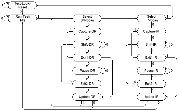
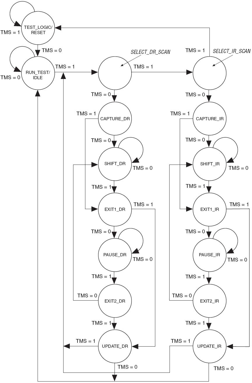
Each JTAG enabled chip has a TAP controller with a state machine with 16 states.
The state of the TMS pin at each TCK pulse dictates the transitions between states.
These states help control whether you are shifting through
the instruction register or one of the data register and
control the capture of data into the shift registers and
latching of data from them.
Here is a diagram of the TAP controller state machine,
produced using graphviz (requires browser/plugin SVG support):

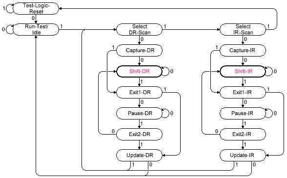
Each ellipse denotes a state and each arrow denotes a transition from one state to another.
There are two transitions from each state, one taken when TMS=0 and one taken when TMS=1.
The shift IR and Shift DR states are emphasized because
that is where you will spend the most time (other than when idle).
These are the states where data is shifted in on TDI and out on TDO
and the machine will stay in those states as long as TMS=0.
The Exit* and Pause* states are not terribly interesting.
For either the data or instruction registers, you usually start by passing through
the Capture_* state which loads data from the chip into the register,
proceed to the shift* state where the captured data is shifted out
while the new data from the PC is shifted in, and then make your way
through a couple minor states to the update state where the new data is latched into the chip.
Here is the TAP controller state machine as a table, which is easily converted into C, VHDL, Verilog, or other languages.
| Current State | TMS=0 | TMS=1 |
| Test-Logic-Reset | Run-Test/Idle | (no change) |
| Run-Test/Idle | (no change) | Select-DR-Scan |
| Select-DR-Scan | Capture-DR | Select-IR-Scan |
| Capture-DR | Shift-DR | Exit1-DR |
| Shift-DR | (no change) | Exit1-DR |
| Exit1-DR | Pause-DR | Update-DR |
| Pause-DR | (no change) | Exit2-DR |
| Exit2-DR | Shift-DR | Update-DR |
| Update-DR | Run-Test/Idle | Select-DR-Scan |
| Select-IR-Scan | Capture-IR | Test-Logic-Reset |
| Capture-IR | Shift-IR | Exit1-IR |
| Shift-IR | (no change) | Exit1-IR |
| Exit1-IR | Pause-IR | Update-IR |
| Pause-IR | (no change) | Exit2-IR |
| Exit2-IR | Shift-IR | Update-IR |
| Update-IR | Run-Test/Idle | Select-DR-Scan |
Note that aside from the first two states, the remaining states are divided into two sets of 7 states
which are almost identical except that one set deals with the instruction register
and one deals with the data register.
These two sets of states deal with three operations:
capture, shift, and update.
Capture loads data from the chip into the corresponding register.
Data is latched on the rising edge of TCK when exiting the capture state.
Shift moves the data out through TDO while new data is shifted in on the TDI pin.
The update-xx states cause the data from the shift register
to be transfered to the selected register.
The update occurs on the falling edge of TCK while still in the update state.
The state machines main states are reset, run/idle, shift DR, and shift IR.
Data is shifted in on the rising edge of TCK and
data out becomes valid on the falling edge of TCK (to be latched on the rising edge).
I.E. Rising edge is the active edge for input and output and
the transitions occur at the falling edge.
TMS=0 to keep the controller in the shift-xx state until all the data is shifted out;
TMS=1 when the last bit is shifted.
Five TCKs with TMS high will reset the state machine
to the Test-Logic-Reset state from any other state.
#define TAP_TEST_LOGIC_RESET 0
#define TAP_RUN_TEST_IDLE 8
#define TAP_SELECT_DR_SCAN 1
#define TAP_CAPTURE_DR  2
#define TAP_SHIFT_DR 3
#define TAP_EXIT1_DR 4
#define TAP_PAUSE_DR 5
#define TAP_EXIT2_DR 6
#define TAP_UPDATE_DR 7
#define TAP_SELECT_IR_SCAN 9
#define TAP_CAPTURE_IR 10
#define TAP_SHIFT_IR 11
#define TAP_EXIT1_IR 12
#define TAP_PAUSE_IR 13
#define TAP_EXIT2_IR 14
#define TAP_UPDATE_IR 15

int jtag_tap_controller_state_machine( int tms )
{
  static int state = TAP_TEST_LOGIC_RESET;
  int nextstate;
  switch ( state )
  {
    case ( TAP_TEST_LOGIC_RESET ):
      if ( !tms )
      {
        nextstate = TAP_RUN_TEST_IDLE;
      }
      else
      {
      }
      break;
    case ( TAP_RUN_TEST_IDLE ):
      if ( !tms )
      {
      }
      else
      {
        nextstate = TAP_SELECT_DR_SCAN;
      }
      break;
    case ( TAP_SELECT_DR_SCAN ):
      if ( !tms )
      {
        nextstate = TAP_CAPTURE_DR;
      }
      else
      {
        nextstate = TAP_SELECT_IR_SCAN;
      }
      break;
    case ( TAP_CAPTURE_DR ):
      if ( !tms )
      {
        nextstate = TAP_SHIFT_DR;
      }
      else
      {
        nextstate = TAP_EXIT1_DR;
      }
      break;
    case ( TAP_SHIFT_DR ):
      if ( !tms )
      {
        ;
      }
      else
      {
        nextstate = TAP_EXIT1_DR;
      }
      break;
    case ( TAP_EXIT1_DR ):
      if ( !tms )
      {
        nextstate = TAP_PAUSE_DR;
      }
      else
      {
        nextstate = TAP_UPDATE_DR;
      }
      break;
    case ( TAP_PAUSE_DR ):
      if ( !tms )
      {
        ;
      }
      else
      {
        nextstate = TAP_EXIT2_DR;
      }
      break;
    case ( TAP_EXIT2_DR ):
      if ( !tms )
      {
        nextstate = TAP_SHIFT_DR;
      }
      else
      {
        nextstate = TAP_UPDATE_DR;
      }
      break;
    case ( TAP_UPDATE_DR ):
      if ( !tms )
      {
        nextstate = TAP_RUN_TEST_IDLE;
      }
      else
      {
        nextstate = TAP_SELECT_DR_SCAN;
      }
      ;
      break;
    case ( TAP_SELECT_IR_SCAN ):
      if ( !tms )
      {
        nextstate = TAP_CAPTURE_IR;
      }
      else
      {
        nextstate = TAP_TEST_LOGIC_RESET;
      }
      break;
    case ( TAP_CAPTURE_IR ):
      if ( !tms )
      {
        nextstate = TAP_SHIFT_IR;
      }
      else
      {
        nextstate = TAP_EXIT1_IR;
      }
      break;
    case ( TAP_SHIFT_IR ):
      if ( !tms )
      {
        ;
      }
      else
      {
        nextstate = TAP_EXIT1_IR;
      }
      break;
    case ( TAP_EXIT1_IR ):
      if ( !tms )
      {
        nextstate = TAP_PAUSE_IR;
      }
      else
      {
        nextstate = TAP_UPDATE_IR;
      }
      break;
    case ( TAP_PAUSE_IR ):
      if ( !tms )
      {
        ;
      }
      else
      {
        nextstate = TAP_EXIT2_IR;
      }
      break;
    case ( TAP_EXIT2_IR ):
      if ( !tms )
      {
        nextstate = TAP_SHIFT_IR;
      }
      else
      {
        nextstate = TAP_UPDATE_IR;
      }
      break;
    case ( TAP_UPDATE_IR ):
      if ( !tms )
      {
        nextstate = TAP_RUN_TEST_IDLE;
      }
      else
      {
        nextstate = TAP_SELECT_DR_SCAN;
      }
      break;
    default:
      nextstate = TAP_TEST_LOGIC_RESET;
  }
  state = nextstate;
  return ( state );
}
his code is an example, intended for illustrations, it hasn't been tested.
"enum" types may be used instead of "#define".
This function should be called once on the rising edge of TCK.
While you probably don't want to implement a TAP controller in software
on an actual hardware device (it would be very slow), simulating one is useful
for keeping track of the state of a controller you are talking too,
debugging, educational purposes, etc.
This example can also be pretty easily converted to VHDL or Verilog for synthesis or simulation.
Note that #defined values for the various states were chosen so that the similarly named instructions
(which have similar state transitions) share 3 bits in common to facilitate logic minimization.
IEEE 1149 has the combinatorial form of the state machine logic expressed as a 4 sums of 17 products,
each product having at most 4 inputs. Thus 21 4-input LUTs could be used to implemnt that logic
(about double that when you include the sequential portion).
The instruction Register (required)
The size of the instruction register varies from chip to chip. Minimum is 2 bits. It contains a shift register, a storage register, and decode logic. The value 01 is loaded into the two least significant bits of the instruction shift register during the capture-ir state. The instruction register also functions as a status register. What is loaded into the other bits depends on the chip.
Required Instructions
BYPASS
The bypass instruction is all 1s. The bypass register is loaded with a 0 when the bypass instruction is executed and the chip enters the Shift-DR state. The contents of the bypass register are ignored during an update-DR. With multiple devices in the chain, you can selectively put some devices into bypass mode by loading a bypass instruction into some instruction registers and another instruction, such as sample/preload, into the others.
SAMPLE/PRELOAD
This instruction loads the state of each input pin into the boundary scan register and also the internal logic state of each output pin. This instruction does not interfere with normal functions. Sample and Preload may be separate or combined.
EXTEST
The EXTEST instruction is all zeros.
External test. This does interfere with normal function. It performs an external boundary scan test to test things like chip to chip connections. In EXTEST mode, each Update-DR state causes data in the boundary scan register to be driven to the output pins. The Capture-DR state causes data from the input pins and internal states for the output pins to be loaded into the boundary shift register (similar to sample/preload). Data is shifted on the rising edge of TCK.
Optional Public Instructions
IDCODE (Optional in 1149.1, Required in 1532)
This instruction allows the chip ID code to be read.
USERCODE (Optional in 1149.1, Required in 1532)
INTEST
RUNBIST
ISC_ENABLE
ISC_DISABLE
ISC_PROGRAM
ISC_NOOP
ISC_READ
ISC_ERASE
ISC_DISCHARGE
ISC_PROGRAM_USERCODE
ISC_PROGRAM_DONE
ISC_ERASE_DONE
ISC_PROGRAM_SECURITY
ISC_READ_INFO
ISC_DATA_SHIFT
ISC_ADDRESS_SHIFT
ISC_INCREMENT
ISC_SETUP
PROBE (1149.4)
EXTEST_PULSE(1149.6)
EXTEST_TRAIN(1149.6)
Other
Additional part specific instructions can be defined. These can be used for things like built in self test, programming flash memory, and On Chip Debug.
Private Instructions
Presumably used for things like factory test. If a chip has, for example, a CPU, RAM, FLASH, FPGA, IO, and bus interconnect blocks, there may be separate or combined scan chains around each block. With a block, there may be internal cells used to further partition the logic into testable domains.
A JTAG device contains multiple registers or chains accessable via the TAP port. If the TAP controller is in the Shift-IR state, the instruction register will be used. In the Shift-DR, the register inserted into the chain will depend on the currently active instruction in the instruction register.
Standard Data Registers
In addition, to the instruction register, each device has more than one data register. At any given time, data is shifted though either the instruction register or one of the data registers depending on the state of the TAP controller and the last instruction loaded. Registers are shifted LSB first.
The boundary-scan register (required)
The boundary-scan register typically contains one or more bits for each logic pin on the device. More than one bit is needed to deal with output enables and direction controls for some pins. All device inputs must be observable and all device outputs controllable through the boundary scan register. The register may provide access to internal states associated with each pin.
The bypass Register (required)
This is a single bit wide shift register connecting TDI and TDO. It is selected in bypass mode and is used to minimize the number of bits that need to be shifted when accessing other chips. Why a one bit delay? Without it, you would end up with an analog delay in TDI proportional to the number of chips and under some conditions, TCK would get there before TDI would.
Device ID register (optional)
This is a 32 bit register that contains information that can be used to identify the specific chips in the chain.
User-Defined (optional)


http://www.fpga4fun.com/JTAG2.html
http://www.freescale.com/webapp/sps/site/overview.jsp?code=784_LPBBJTAGTAP
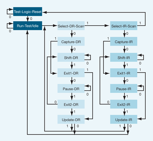
Figure 1: TAP Controller State Diagram
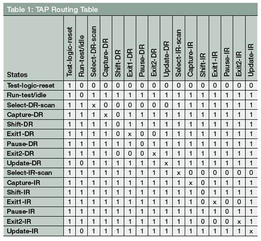
As a result, it is sufficient for any of the shortest paths starting at s1 and ending at sn to store the very next state following the state s1 on the path. The repository that stores the very next state for each of the shortest paths is called a routing table, similarly defined in networks to route messages. Unlike networks where every node stores a vector of the very next nodes, our routing table is a matrix because the traversing is controlled via the TAP interface. The TAP routing table is depicted in Table 1.
