

(筆記) 如何設計邊緣檢測電路? (SOC) (Verilog)
Abstract
邊緣檢測電路(edge detection circuit)是個常見的基本電路。
Introduction
使用環境:Quartus II 7.2 SP3
所謂的邊緣檢測,簡單的說就是判斷前一個clock的狀態和目前clock狀態的比較,若由0變1,就是上升沿檢測電路(posedge edge detection circuit)(又稱上緣微分電路),若是由1變0,就是下升沿檢測電路(negedge edge detection circuit)(又稱下緣微分電路),若上升沿與下升沿都要檢測,就是雙沿檢測電路電路(double edge detection)。
上升沿檢測電路(posedge detection circuit)
Method 1:
使用兩個reg
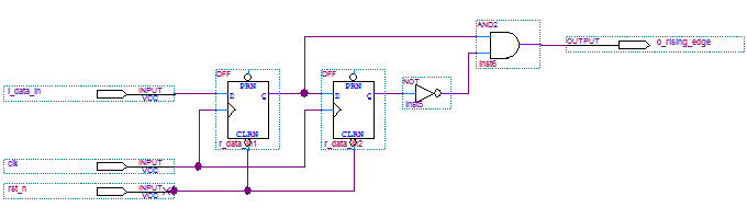
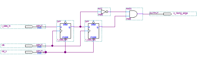
r_data_in0與r_data_in1為D-FF,分別hold住上一個clock與目前clock的i_data_in,所謂上升沿電路,就是i_data_in由0變1,也就是r_data_in0為0且r_data_in1為1,故用not接r_data_in0,之後再用and連接r_data_in1。
posedge_detection.v / Verilog

2 (C) OOMusou 2008 http://oomusou.cnblogs.com
3
4 Filename : posedge_detection.v
5 Compiler : Quartus II 7.2 SP3
6 Description : Demo how to design posedge detection circuit
7 Release : 07/06/2008 1.0
8 */
9
10 module posedge_detection (
11 input clk,
12 input rst_n,
13 input i_data_in,
14 output o_rising_edge
15 );
16
17 reg r_data_in0;
18 reg r_data_in1;
19
20 assign o_rising_edge = ~r_data_in0 & r_data_in1;
21
22 always@(posedge clk, negedge rst_n) begin
23 if (!rst_n) begin
24 r_data_in0 <= 0;
25 r_data_in1 <= 0;
26 end
27 else begin
28 r_data_in0 <= r_data_in1;
29 r_data_in1 <= i_data_in;
30 end
31 end
32
33 endmodule
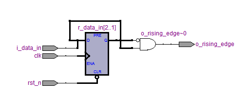
這種寫法經過合成後,會很聰明的只用一個2 bit的D-FF,與一個AND。
Method 2:
使用1個reg
posedge_edgedetection2.v / Verilog
2 (C) OOMusou 2008 http://oomusou.cnblogs.com
3
4 Filename : posedge_detection2.v
5 Compiler : Quartus II 7.2 SP3
6 Description : Demo how to design posedge detection circuit
7 Release : 08/11/2008 1.0
8 */
9
10 module posedge_detection2 (
11 input clk,
12 input rst_n,
13 input i_data_in,
14 output reg o_rising_edge
15 );
16
17 reg r_data_in0;
18
19 always@(posedge clk, negedge rst_n) begin
20 if (!rst_n)
21 r_data_in0 <= 0;
22 else begin
23 r_data_in0 <= i_data_in;
24
25 if ({r_data_in0, i_data_in} == 2'b01)
26 o_rising_edge <= 1;
27 else
28 o_rising_edge <= 0;
29 end
30 end
31
32 endmodule
若你覺得Method 1比較不好理解,那Method 2就非常的behavior,只使用一個reg記住前一個clock的狀態,並在這個clock判斷前一個狀態是否為0且目前狀態是否為1,這樣就是posedge了。
這種寫法經過合成之後,只有一個D-FF與EQUAL,右邊的o_rising_edge的D-FF主要是因為在always block內的reg。

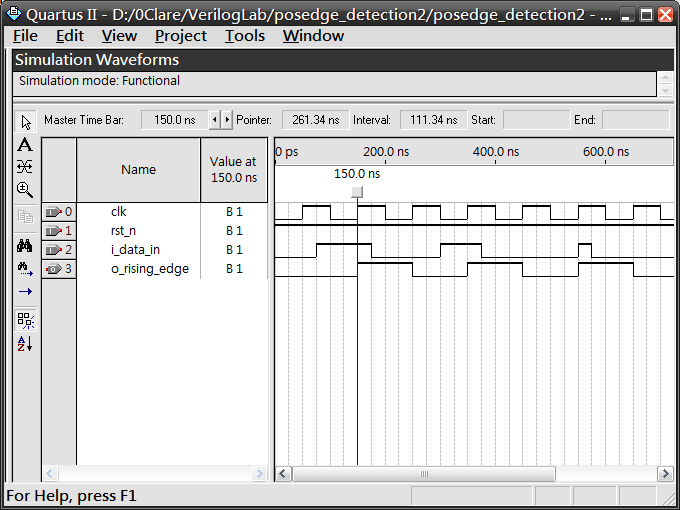
就這個例子而言,Method 1與Method 2目前在Quartus II 7.2 SP3的合成下resource打成平手,logic element各用兩個D-FF與與一個組合電路,不過Method 2的code可讀性比較高。

下升沿檢測電路(negedge detection circuit)
r_data_in2與r_data_in1為reg,分別hold住上一個clock與目前clock的i_data_in,所謂下升沿電路,就是i_data_in由1變0,也就是r_data_in2為1且r_data_in1為0,故用not接r_data_in1,之後再用and連接r_data_in2。
Method 1:
使用兩個reg
nededge_detection.v / Verilog
2 (C) OOMusou 2008 http://oomusou.cnblogs.com
3
4 Filename : nededge_detection.v
5 Compiler : Quartus II 7.2 SP3
6 Description : Demo how to design nededge detection circuit
7 Release : 07/06/2008 1.0
8 */
9 module negedge_detection (
10 input clk,
11 input rst_n,
12 input i_data_in,
13 output o_falling_edge
14 );
15
16 reg r_data_in0;
17 reg r_data_in1;
18
19 assign o_falling_edge = r_data_in0 & ~r_data_in1;
20
21 always@(posedge clk, negedge rst_n) begin
22 if (!rst_n) begin
23 r_data_in0 <= 0;
24 r_data_in1 <= 0;
25 end
26 else begin
27 r_data_in0 <= r_data_in1;
28 r_data_in1 <= i_data_in;
29 end
30 end
31
32 endmodule
Method 2:
使用1個reg
nededge_detection2.v
2 (C) OOMusou 2008 http://oomusou.cnblogs.com
3
4 Filename : nededge_detection2.v
5 Compiler : Quartus II 7.2 SP3
6 Description : Demo how to design nededge detection circuit
7 Release : 07/06/2008 1.0
8 */
9 module negedge_detection2 (
10 input clk,
11 input rst_n,
12 input i_data_in,
13 output reg o_falling_edge
14 );
15
16 reg r_data_in0;
17
18 always@(posedge clk, negedge rst_n) begin
19 if (!rst_n)
20 r_data_in0 <= 0;
21 else begin
22 r_data_in0 <= i_data_in;
23
24 if ({r_data_in0, i_data_in} == 2'b10)
25 o_falling_edge <= 1;
26 else
27 o_falling_edge <= 0;
28 end
29 end
30
31 endmodule


雙沿檢測電路電路(double edge detection)

r_data_in2與r_data_in1為reg,分別hold住上一個clock與目前clock的i_data_in,所謂雙沿電路,就是i_data_in由1變0,或者由0變1,也就是r_data_in2為1且r_data_in1為0,或者r_data_in2為0且r_data_in1為1時,故用xor接r_data_in1與r_data_in2。
Method 1:
使用2個reg
doubleedge_detection.v / Verilog
2 (C) OOMusou 2008 http://oomusou.cnblogs.com
3
4 Filename : doubleedge_detection.v
5 Compiler : Quartus II 7.2 SP3
6 Description : Demo how to design double edge detection circuit
7 Release : 07/06/2008 1.0
8 */
9
10 module doubleedge_detection (
11 input clk,
12 input rst_n,
13 input i_data_in,
14 output o_double_edge
15 );
16
17 reg r_data_in0;
18 reg r_data_in1;
19
20 assign o_double_edge = r_data_in0 ^ r_data_in1;
21
22 always@(posedge clk, negedge rst_n) begin
23 if (!rst_n) begin
24 r_data_in0 <= 0;
25 r_data_in1 <= 0;
26 end
27 else begin
28 r_data_in0 <= r_data_in1;
29 r_data_in1 <= i_data_in;
30 end
31 end
32
33 endmodule
Method 2:
使用1個reg
doubleedge_detection2.v / Verilog
2 (C) OOMusou 2008 http://oomusou.cnblogs.com
3
4 Filename : doubleedge_detection2.v
5 Compiler : Quartus II 7.2 SP3
6 Description : Demo how to design double edge detection circuit
7 Release : 07/06/2008 1.0
8 */
9
10 module doubleedge_detection2 (
11 input clk,
12 input rst_n,
13 input i_data_in,
14 output reg o_double_edge
15 );
16
17 reg r_data_in0;
18
19 always@(posedge clk, negedge rst_n) begin
20 if (!rst_n)
21 r_data_in0 <= 0;
22 else begin
23 r_data_in0 <= i_data_in;
24
25 if ({r_data_in0, i_data_in} == 2'b10)
26 o_double_edge <= 1;
27 else if ({r_data_in0, i_data_in} == 2'b01)
28 o_double_edge <= 1;
29 else
30 o_double_edge <= 0;
31
32 // another method
33 // o_double_edge <= r_data_in0 ^ i_data_in;
34 end
35 end
36
37 endmodule


完整程式碼下載
posedge_detection.7z
posedge_detection2.7z
negedge_detection.7z
negedge_detection2.7z
doubleedge_detection.7z
doubleedge_detection2.7z
Conclusion
什麼時候會使用這種電路呢?若input是非同步信號,為了要讓input與你同步的FSM一起處理,必須先經過邊緣檢測,使之與clock同步,然後才能跟你的FSM一起運作。
See Also
(原創) 如何使用ModelSim-Altera作電路模擬? (SOC) (Quartus II) (ModelSim)
(筆記) 如何以絕對時間指定testbench波形? (SOC) (Verilog)
(原創) 深入探討Altera的Checksum Master範例 (SOC) (SOPC Builder) (Nios II) (DE2)
Reference
王钿、卓興旺 2007,基於Verilog HDL的數字應用設計,國防工業出版社


【推荐】还在用 ECharts 开发大屏?试试这款永久免费的开源 BI 工具!
【推荐】国内首个AI IDE,深度理解中文开发场景,立即下载体验Trae
【推荐】编程新体验,更懂你的AI,立即体验豆包MarsCode编程助手
【推荐】抖音旗下AI助手豆包,你的智能百科全书,全免费不限次数
【推荐】轻量又高性能的 SSH 工具 IShell:AI 加持,快人一步